„Spintronika” változatai közötti eltérés
(Új oldal, tartalma: „ ==Bevezetés== <wlatex> The spin dependence of electronic transport is hidden in most metals. However, spin polarized current injected to a nonmagnetic conductor keeps t…”) |
(→Bevezetés) |
||
| 27. sor: | 27. sor: | ||
technical application and trigger an intensive development of novel memory | technical application and trigger an intensive development of novel memory | ||
elements. | elements. | ||
| − | < | + | </wlatex> |
==Spinpolarizált vezetés nanoszerkezetekben== | ==Spinpolarizált vezetés nanoszerkezetekben== | ||
<wlatex> | <wlatex> | ||
| 271. sor: | 271. sor: | ||
situation where the current spin polarization may take a sign opposite to that | situation where the current spin polarization may take a sign opposite to that | ||
of the magnetization (Fig.~\ref{DOS}b). | of the magnetization (Fig.~\ref{DOS}b). | ||
| − | |||
| − | |||
| − | |||
| − | |||
| − | |||
| − | |||
| − | |||
| − | |||
| − | |||
| − | |||
| − | |||
| − | |||
| − | |||
| − | |||
| − | |||
| − | |||
| − | |||
| − | |||
| − | |||
| − | |||
| − | |||
| − | |||
| − | |||
| − | |||
| − | |||
| − | |||
| − | |||
| − | |||
| − | |||
| − | |||
| − | |||
| − | |||
| − | |||
| − | |||
| − | |||
| − | |||
| − | |||
| − | |||
| − | |||
| − | |||
| − | |||
| − | |||
| − | |||
| − | |||
| − | |||
| − | |||
| − | |||
| − | |||
| − | |||
| − | |||
| − | |||
| − | |||
| − | |||
| − | |||
| − | |||
| − | |||
| − | |||
| − | |||
| − | |||
| − | |||
| − | |||
| − | |||
| − | |||
| − | |||
| − | |||
| − | |||
| − | |||
| − | |||
| − | |||
| − | |||
| − | |||
| − | |||
| − | |||
| − | |||
| − | |||
| − | |||
| − | |||
| − | |||
| − | |||
| − | |||
| − | |||
| − | |||
| − | |||
| − | |||
| − | |||
| − | |||
| − | |||
| − | |||
| − | |||
| − | |||
| − | |||
| − | |||
| − | |||
| − | |||
| − | |||
| − | |||
| − | |||
| − | |||
| − | |||
| − | |||
| − | |||
| − | |||
| − | |||
| − | |||
| − | |||
| − | |||
| − | |||
| − | |||
| − | |||
| − | |||
| − | |||
| − | |||
| − | |||
| − | |||
| − | |||
| − | |||
| − | |||
| − | |||
| − | |||
| − | |||
| − | |||
| − | |||
| − | |||
| − | |||
| − | |||
| − | |||
| − | |||
| − | |||
| − | |||
| − | |||
| − | |||
| − | |||
| − | |||
| − | |||
| − | |||
| − | |||
| − | |||
| − | |||
| − | |||
| − | |||
| − | |||
| − | |||
| − | |||
| − | |||
| − | |||
| − | |||
| − | |||
| − | |||
| − | |||
| − | |||
| − | |||
| − | |||
| − | |||
| − | |||
| − | |||
| − | |||
| − | |||
| − | |||
| − | |||
| − | |||
| − | |||
| − | |||
| − | |||
| − | |||
| − | |||
| − | |||
| − | |||
| − | |||
| − | |||
| − | |||
| − | |||
| − | |||
| − | |||
| − | |||
| − | |||
| − | |||
| − | |||
| − | |||
| − | |||
| − | |||
| − | |||
| − | |||
| − | |||
| − | |||
| − | |||
| − | |||
| − | |||
\section{The spin valve structure} | \section{The spin valve structure} | ||
| 642. sor: | 455. sor: | ||
overview on spin valve applications was given. | overview on spin valve applications was given. | ||
| − | + | </wlatex> | |
| − | + | ||
| − | + | ||
| − | + | ||
| − | + | ||
| − | + | ||
| − | + | ||
| − | + | ||
| − | + | ||
| − | + | ||
| − | + | ||
| − | + | ||
| − | + | ||
| − | + | ||
| − | + | ||
| − | + | ||
| − | + | ||
| − | + | ||
| − | + | ||
| − | + | ||
| − | < | + | |
A lap 2013. június 28., 06:35-kori változata
Bevezetés
The spin dependence of electronic transport is hidden in most metals. However,
spin polarized current injected to a nonmagnetic conductor keeps the spin memory
within a certain distance, typically in the submicron range. By now, nanoscale
devices have been prepared where the size of the components is well below the
distance of the spin-memory, and both the control of the spin states and the
utilization of the spin information have been
demonstrated.\cite{Wolf16112001,Awschalom2007} In most of these electronic
applications ferromagnetic components act as spin filter and detector,
\cite{RevModPhys.76.323,0022-3727-35-18-201} while a nonmagnetic metal mediates
the spin information: this is the simplest spin-valve structure. For the design
of such nanodevices a proper understanding of spin dependent transport is
necessary, including the knowledge of the carriers' spin-polarization, or the
determination of the spin diffusion length.
In the first part of this review we present a simple model for the spin dependent transmission through a nanostructure based on the Landauer formalism widely applied in the field of nanophysics. In the second part a special measurement technique is reviewed, which allows the direct determination of the current spin polarization, and with which even the decay of the spin polarization i.e.~the spin diffusion length can be determined in a nonmagnetic layer. In the last part the nanoscale spin-valve architecture is discussed, demonstrating how the results of basic research find broad technical application and trigger an intensive development of novel memory elements.
Spinpolarizált vezetés nanoszerkezetekben
In a macroscopic conductor the electrons suffer numerous scattering processes as
they move from one electrode towards the other. Due to the scattering on
impurities and lattice defects the drift momentum of the electrons gained from
the electric field is lost. This process is described by the characteristic
length scale of the momentum relaxation mean free path,  . Inelastic
scattering processes like the scattering on lattice vibrations lead to a change
of energy, which results in the loss of phase coherence for electron waves. The
corresponding characteristic length scale is called phase diffusion length,
. Inelastic
scattering processes like the scattering on lattice vibrations lead to a change
of energy, which results in the loss of phase coherence for electron waves. The
corresponding characteristic length scale is called phase diffusion length,
 .\cite{nazarov_book,datta_book} Within a large enough distance the
electrons also loose their spin information, as characterized by the spin diffusion length,
.\cite{nazarov_book,datta_book} Within a large enough distance the
electrons also loose their spin information, as characterized by the spin diffusion length,
 .\cite{RevModPhys.76.323,fabian:1708} In a nanostructure, however, all
these length scales may become comparable to, or even larger than the characteristic size of the structure,
.\cite{RevModPhys.76.323,fabian:1708} In a nanostructure, however, all
these length scales may become comparable to, or even larger than the characteristic size of the structure,
 . For instance, in small enough structures (
 ) the spin information is
preserved, which is a key ingredient for spintronic
applications.\cite{PhysRevB.48.7099} For structures smaller than
coherent quantummechanical features appear, whereas for
) the spin information is
preserved, which is a key ingredient for spintronic
applications.\cite{PhysRevB.48.7099} For structures smaller than
coherent quantummechanical features appear, whereas for  a ballistic
transport is observed, i.e.~the electrons scatter only on the edges of the
structure, but not inside.
a ballistic
transport is observed, i.e.~the electrons scatter only on the edges of the
structure, but not inside.
Here we give a simple model to demonstrate how spin-polarized current may arise in ferromagnetic nanostructures, which are smaller than the spin diffusion length. In order to provide a microscopic insight to the relevant processes we use the well established approach of the Landauer formalism,\cite{Landauer_form,datta_book} which has been successfully applied to describe several nanoscale systems, like atomic-sized conductors\cite{Agrait200381} or semiconductor nanostructures.\cite{PhysRevLett.60.848,ihn_book}
\begin{figure} [!h]
\centering
\includegraphics[width=0.7\columnwidth]{fig1.eps}
\caption{\it Panel (a) demonstrates an ideal 2D quantum wire with parallel
walls and the absence of scattering inside the wire. The standing waves
demonstrate the quantized transverse modes in the wire. Panel (b) demonstrates
the dispersion of the conductance channels inside the wire in a free electron
picture. The blue parabolas correspond to spin up electrons, whereas the red
parabolas stand for the spin down electrons. The two spin subbands are shifted
by an energy  . The thick/thin lines denote the
occupied/unoccupied states. Note, that right going states (
. The thick/thin lines denote the
occupied/unoccupied states. Note, that right going states ( ) are occupied
up to an energy higher by
) are occupied
up to an energy higher by  than the left moving states (
 ).}
\label{Qwire}
\end{figure}
).}
\label{Qwire}
\end{figure}
As a simplified model first we consider an ideal two dimensional wire with
parallel walls (Fig.~\ref{Qwire}(a)). In the ballistic limit no scattering occurs
in the wire, and an electron entering into the wire from one side will propagate
to the other side without changing its energy and spin state. Along
the wire ( -direction) the electrons exhibit a free, reflectionless
propagation, whereas perpendicular to the wire (
-direction) the electrons exhibit a free, reflectionless
propagation, whereas perpendicular to the wire ( -direction) quantized
transverse modes are formed. In this simple geometry the wavefunction factorizes
to the product of a longitudinal and a transverse wave function, and the
energies corresponding to the transverse standing waves and the longitudinal
propagation are simply added. After including magnetism in a Stoner type picture
the energy dispersion for this system can be written as:
\begin{equation}
\varepsilon_n^{\sigma}(k)=\varepsilon(k)+\varepsilon_n-\sigma\varepsilon_{\mathrm{ex}},
\end{equation}
where
-direction) quantized
transverse modes are formed. In this simple geometry the wavefunction factorizes
to the product of a longitudinal and a transverse wave function, and the
energies corresponding to the transverse standing waves and the longitudinal
propagation are simply added. After including magnetism in a Stoner type picture
the energy dispersion for this system can be written as:
\begin{equation}
\varepsilon_n^{\sigma}(k)=\varepsilon(k)+\varepsilon_n-\sigma\varepsilon_{\mathrm{ex}},
\end{equation}
where  is the energy corresponding to the quantized transverse
modes,
is the energy corresponding to the quantized transverse
modes,  is the dispersion of the extended Bloch states in the
direction (
is the dispersion of the extended Bloch states in the
direction ( =
= ),
),  is the spin index, and
 is the exchange energy. The resulting dispersion is a
set of one dimensional dispersion curves, which are vertically shifted by the
transverse energies and the exchange energy (Fig.~\ref{Qwire}(b)). The discrete
one dimensional dispersions are called \emph{conductance
channels}.\cite{PhysRevB.31.6207,datta_book}
is the exchange energy. The resulting dispersion is a
set of one dimensional dispersion curves, which are vertically shifted by the
transverse energies and the exchange energy (Fig.~\ref{Qwire}(b)). The discrete
one dimensional dispersions are called \emph{conductance
channels}.\cite{PhysRevB.31.6207,datta_book}
In such an ideal wire the states with positive and negative are well
separated, the former are all coming from the left electrode, while the latter are all
coming from the right electrode. In a symmetric situation no net current flows.
Application of a bias voltage between the two sides of the wire, however, shifts
the chemical potentials of the right and left moving electron states by
with respect to each other, and this imbalance results in a finite current. For
a selected conductance channel the velocity of the electrons and the density of
states is respectively given as
\begin{equation}
v_n^{\sigma}=\frac{1}{\hbar}\frac{\partial \varepsilon_n^{\sigma}(k)}{\partial k},\ \ \ \ g_n^{\sigma}=\frac{L}{2\pi}\left(\frac{\partial \varepsilon_n^{\sigma}(k)}{\partial k}\right)^{-1},
\label{vn}
\end{equation}
where is the length of the nanowire. The spacial density for the electron
states in the energy window is obtained as
\begin{equation}
n_n^{\sigma}=eV g_n^{\sigma}/L.
\end{equation}
The current is then calculated as a product of charge, velocity and electron
density, summing over the spins and all the conductance channels:
\begin{equation}
I=\sum_\sigma \sum_{n=1}^{M^{\sigma}}e v_n^{\sigma} n_n^{\sigma} =\sum_\sigma\frac{e^2}{h}M^{\sigma}V.
\end{equation}
Here  is the number of open conductance channels, i.e. the number of
1D dispersion curves crossing the Fermi energy for a given spin orientation.
Note that
is the number of open conductance channels, i.e. the number of
1D dispersion curves crossing the Fermi energy for a given spin orientation.
Note that  cancels in the product of
  and
and
 , thus the above result is valid for any shape of the dispersion curve.
Furthermore, the two dimensional model only simplifies the visualization, but
the above arguments also hold for any perfect three dimensional nanowire with
uniform cross section along the axis.
, thus the above result is valid for any shape of the dispersion curve.
Furthermore, the two dimensional model only simplifies the visualization, but
the above arguments also hold for any perfect three dimensional nanowire with
uniform cross section along the axis.
Here we have taken advantage of the assumption that the spin state is conserved,
i.e. the structure is smaller than the spin diffusion length. This has allowed
the separation of the current to a purely spin up and a purely spin down component
being two independent \emph{routes} of the transport:
 . The
total current is determined by the number of open conductance channels, and the
conductance (
. The
total current is determined by the number of open conductance channels, and the
conductance ( ) is an integer multiple of
  k
k .
.
\begin{figure} [!h] \centering \includegraphics[width=\columnwidth]{fig2.eps} \caption{\it The dispersion curves around the Fermi energy for the different conductance channels. The bottom and top panels correspond to spin up and spin down electrons, respectively. Due to the exchange splitting the number of open conductance channels differs for the two spin subbands.} \label{linear} \end{figure}
Due to the shifted spin subbands,  not necessarily equals
 . This is indicated by Fig.~\ref{linear}, where only the
linearized part of the 1D dispersions around the Fermi energy is shown
demonstrating that the free electron dispersions in Fig.~\ref{Qwire}(b) are only
illustrations and are generally not considered in this model. The degree of the
resulting spin polarization can be characterized by the ratio of the spin
polarized current and the total current:
\begin{equation}
P_c=\frac{I^{\uparrow}-I^{\downarrow}}{I^{\uparrow}+I^{\downarrow}}=\frac{M^{\uparrow}-M^{\downarrow}}{M^{\uparrow}+M^{\downarrow}}.
\label{Pc}
\end{equation}
This normalized current spin polarization can reach even
. This is indicated by Fig.~\ref{linear}, where only the
linearized part of the 1D dispersions around the Fermi energy is shown
demonstrating that the free electron dispersions in Fig.~\ref{Qwire}(b) are only
illustrations and are generally not considered in this model. The degree of the
resulting spin polarization can be characterized by the ratio of the spin
polarized current and the total current:
\begin{equation}
P_c=\frac{I^{\uparrow}-I^{\downarrow}}{I^{\uparrow}+I^{\downarrow}}=\frac{M^{\uparrow}-M^{\downarrow}}{M^{\uparrow}+M^{\downarrow}}.
\label{Pc}
\end{equation}
This normalized current spin polarization can reach even  (
( ) in
case of a half-metal, where only one type of carrier is present at the
Fermi level.
) in
case of a half-metal, where only one type of carrier is present at the
Fermi level.
\begin{figure} [!h] \centering \includegraphics[width=0.7\columnwidth]{fig3.eps} \caption{\it A diffusive ferromagnetic region is sandwiched between two normal metal ideal quantum wires. The transport is determined by spin dependent transmission probabilities between the conductance channels at the two sides.} \label{landauer} \end{figure}
A more realistic description can be given for the conductance of a piece of
magnetic nanowire inserted between nonmagnetic reservoirs by taking also into
account elastic scatterings (Fig.~\ref{landauer}). According to the Landauer
picture the transport in this system can be be described by the transmission
probabilities  , i.e. the probability for the transmission of an electron
from channel on the left side to channel
, i.e. the probability for the transmission of an electron
from channel on the left side to channel  on the right side. These
transmission probabilities depend on the ``waveguide parameters of the wire.
While
on the right side. These
transmission probabilities depend on the ``waveguide parameters of the wire.
While  corresponds to the previous model of an ideal wire,
 represents scatterings in the wire due to defects, impurities, etc.
As no spin mixing occurs between the spin up and spin down states, the current
can still be calculated for each spin state independently taking into account
the finite transmissions of the
channels:\cite{PhysRevB.31.6207,Agrait200381,datta_book}
\begin{equation}
I^\sigma=\frac{e^2}{h}\sum_{n,m=1}^{M^\sigma}T_{nm}^\sigma V.
\end{equation}
The values of depend on the Fermi wave numbers of the involved
channels. Due to the spin-dependent shift of the dispersions the spin up and the
spin down channels have different wave numbers at the Fermi energy. Thus, in
general, the transmission probability may become spin dependent even without any
direct spin-interaction, like spin-orbit coupling.
The spin dependent current can be rewritten in the form:
\begin{equation}
I^\sigma=\frac{e^2}{h}M^\sigma \bar{T}^\sigma V,
\end{equation}
where  is the average transmission probability for all the
conductance channels with a given spin direction. With this notation the spin
polarization of the current can be written as:
\begin{equation}
P_c=\frac{I^{\uparrow}-I^{\downarrow}}{I^{\uparrow}+I^{\downarrow}}=\frac{M^{\uparrow}\bar{T}^\uparrow-M^{\downarrow}\bar{T}^\downarrow}{M^{\uparrow}\bar{T}^\uparrow+M^{\downarrow}\bar{T}^\downarrow}.
\end{equation}
It is evident from this formula, that either the difference of the transmission
probabilities for the two spin channels, or the difference in the number of open
channels for spin up and spin down electrons gives contribution to the spin
polarization of the current.
is the average transmission probability for all the
conductance channels with a given spin direction. With this notation the spin
polarization of the current can be written as:
\begin{equation}
P_c=\frac{I^{\uparrow}-I^{\downarrow}}{I^{\uparrow}+I^{\downarrow}}=\frac{M^{\uparrow}\bar{T}^\uparrow-M^{\downarrow}\bar{T}^\downarrow}{M^{\uparrow}\bar{T}^\uparrow+M^{\downarrow}\bar{T}^\downarrow}.
\end{equation}
It is evident from this formula, that either the difference of the transmission
probabilities for the two spin channels, or the difference in the number of open
channels for spin up and spin down electrons gives contribution to the spin
polarization of the current.
In case of a few conductance channels the difference in  and
and
 may introduce a spin polarized current even for the same
number of open channels. Indeed, for ferromagnetic atomic point contacts, the
transmission probabilities for the two spin channels are expected to differ
significantly.\cite{PhysRevB.77.104409}
may introduce a spin polarized current even for the same
number of open channels. Indeed, for ferromagnetic atomic point contacts, the
transmission probabilities for the two spin channels are expected to differ
significantly.\cite{PhysRevB.77.104409}
However, for larger structures, where
many conductance channels are present (Fig.~\ref{linear}), is
an average over a broad ensemble of different wavenumbers, and for diffusive
junctions random matrix theory (RMT) predicts a universal value of
\(\bar{T}^{\sigma}=l_m^{\sigma}/L\),\cite{RevModPhys.69.731} where \(L\) is the
length of the diffusive region. As the momentum relaxation
mean free path is expected to be similar for the two spin subbands,  can be assumed. Accordingly the key contribution to the spin
polarization is given solely by the difference of
can be assumed. Accordingly the key contribution to the spin
polarization is given solely by the difference of  and
and  . In this limit, Eq.~\ref{Pc}
gives a reasonable approximation for the spin polarization, even for non-ideal transmission probabilities
(
. In this limit, Eq.~\ref{Pc}
gives a reasonable approximation for the spin polarization, even for non-ideal transmission probabilities
( ).
).
According to Eq.~\ref{vn} the number of conductance channels can be formally
written as:
\begin{equation}
M^\sigma=\frac{2\pi\hbar}{L}\sum_{n=1}^{M^\sigma}v_n^{\sigma}g_n^{\sigma}.
\end{equation}
Introducing a mean Fermi velocity, which is the average of the Fermi velocities for the different conductance channels weighted by the density of states of the channels,
\begin{equation}
\bar{v}_F^\sigma=\frac{\sum_{n} g_n^\sigma v_n^\sigma}{\sum_{n} g_n^\sigma},
\end{equation}
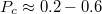
and noting that  is the total density of states at the Fermi level, the formula for the current spin polarization can be rewritten as:
\begin{equation}
P_c\approx\frac{M^{\uparrow}-M^{\downarrow}}{M^{\uparrow}+M^{\downarrow}}=\frac{g_F^{\uparrow}\bar{v}_F^{\uparrow}-g_F^{\downarrow}\bar{v}_F^{\downarrow}}{g_F^{\uparrow}\bar{v}_F^{\uparrow}+g_F^{\downarrow}\bar{v}_F^{\downarrow}}.
\label{PcDOS}
\end{equation}
This formula supplies a microscopic background for the conventional
formulation of the current spin polarization\cite{PhysRevB.70.054416} expressed
by Fermi surface parameters of the two spin subbands: density of states and Fermi velocity.
is the total density of states at the Fermi level, the formula for the current spin polarization can be rewritten as:
\begin{equation}
P_c\approx\frac{M^{\uparrow}-M^{\downarrow}}{M^{\uparrow}+M^{\downarrow}}=\frac{g_F^{\uparrow}\bar{v}_F^{\uparrow}-g_F^{\downarrow}\bar{v}_F^{\downarrow}}{g_F^{\uparrow}\bar{v}_F^{\uparrow}+g_F^{\downarrow}\bar{v}_F^{\downarrow}}.
\label{PcDOS}
\end{equation}
This formula supplies a microscopic background for the conventional
formulation of the current spin polarization\cite{PhysRevB.70.054416} expressed
by Fermi surface parameters of the two spin subbands: density of states and Fermi velocity.
\begin{figure} [!h]
\centering
\includegraphics[width=\columnwidth]{fig4.eps}
\caption{\it Illustration for the density of states in ferromagnets. The
magnetism is related to the exchange splitting of the narrow  (or
(or  )
bands. Panel (a) demonstrates the DOS in Fe: for minority spins (left side) the
band is above the Fermi level, whereas for majority spins (right side) the
Fermi level lies inside the band. Accordingly the DOS is significantly
larger for the majority spins. Panel (b) demonstrates the DOS for Co and Ni type
band filling. In this case
)
bands. Panel (a) demonstrates the DOS in Fe: for minority spins (left side) the
band is above the Fermi level, whereas for majority spins (right side) the
Fermi level lies inside the band. Accordingly the DOS is significantly
larger for the majority spins. Panel (b) demonstrates the DOS for Co and Ni type
band filling. In this case  is above the band for majority
spins, whereas it lies inside the band for minority spins resulting in a
negative Fermi surface spin polarization with respect to the positive
magnetization.}
\label{DOS}
\end{figure}
is above the band for majority
spins, whereas it lies inside the band for minority spins resulting in a
negative Fermi surface spin polarization with respect to the positive
magnetization.}
\label{DOS}
\end{figure}
In real ferromagnets the exchange splitting of narrow (or ) bands and the
filling of the bands determine the magnetic properties (see Fig.~\ref{DOS}). The
integral of the density of states up to the Fermi energy is different for the
two spin orientations, which results in a finite magnetization, conventionally
selecting the up spin as the majority spin orientation. However, the electron
transport is determined by the Fermi surface properties. The spin polarized
transport is not characterized by the magnetization, rather it is described by
the spin polarization of the current as described by Eq.~\ref{PcDOS}. An
interesting example is supplied by the Co or Ni type band fillings: the density
of states at the Fermi level is much larger for the down spin, leading to a
situation where the current spin polarization may take a sign opposite to that
of the magnetization (Fig.~\ref{DOS}b).
\section{The spin valve structure}
The knowledge of current spin polarization and spin diffusion length is essential for the design of spintronic devices. In the previous part we have shown an experimental method which allows the determination of both quantities. In the following we turn to the application of spin polarized transport by discussing the most widely utilized spintronic device, the nanoscale spin-valve structure. First we give simple demonstrative models for this structure, and then we briefly discuss possible applications for next generation data storage devices.
The basic idea of this structure dates back to the discovery of the giant magnetoresistance (GMR) effect by Albert Fert \cite{PhysRevLett.61.2472} and Peter Gr\"unberg \cite{PhysRevB.39.4828}, for which the Nobel price in physics was awarded in 2007. The architecture is based on two ferromagnetic layers, which are separated by a paramagnetic layer being thinner than the spin diffusion length (Fig.~\ref{GMR1}(a)). It was found that the conductance of this device is larger for the parallel orientation of the two magnetic layers than for the antiparallel orientation.
\begin{figure} [!h]
\centering
\includegraphics[width=\columnwidth]{fig9.eps}
\caption{\it Panel (a) demonstrates the basic idea of a spin valve structure:
two ferromagnetic regions are separated by a narrow normal region, and this
structure is connected to normal leads at both sides. Panels (b,d) demonstrate
the variation of the exchange energy along the structure. Panel (b) corresponds
to the parallel magnetic orientation of the layers (both layers have  magnetic orientation), whereas panel (d) demonstrates the antiparallel
orientation ( in the first layer and
magnetic orientation), whereas panel (d) demonstrates the antiparallel
orientation ( in the first layer and  in the second one).
Panels (c) and (e) respectively show the equivalent ballistic model, where the
change of the exchange energy is replaced by an effective narrowing or widening
of the channel.}
\label{GMR1}
\end{figure}
in the second one).
Panels (c) and (e) respectively show the equivalent ballistic model, where the
change of the exchange energy is replaced by an effective narrowing or widening
of the channel.}
\label{GMR1}
\end{figure}
To understand this phenomenon, as the simplest model we can consider an ideal
quantum wire, in which the exchange coupling is switched on adiabatically in two
regions (Fig.~\ref{GMR1}(b,d)). The parallel orientation is modeled by a
positive exchange in both regions, whereas the antiparallel orientation
corresponds to opposite signs of the exchange in the two regions. Similarly to
the previous situations the current can be divided to two independent components
corresponding to spin up and spin down electrons. For a given spin orientation
the effect of the exchange energy is very similar to an effective spatial
narrowing or widening of the channel, which would increase/decrease the
transverse quantized energies (Fig.~\ref{GMR1}(c,e)). Therefore the system can
be considered as serial connected quantum point contacts. For electrons with
majority spin direction (spin direction parallel to the magnetization direction)
the number of open channels is denoted by , whereas for minority
spins (antiparallel spin direction to the magnetization direction) the number of
open channels is  . (Note, that here the superscript
denotes majority orientation instead of the real spin direction,
and the number of open channels is also for down spins in down
oriented magnetization of the magnetic layer.)
. (Note, that here the superscript
denotes majority orientation instead of the real spin direction,
and the number of open channels is also for down spins in down
oriented magnetization of the magnetic layer.)
In such ballistic quantum point contacts the conductance is determined by the
number of modes at the narrowest cross section. If the two magnetic layers have
antiparallel (AP) orientation either the first or the second layer restricts the
number of channels to , and so the conductance for both spin
channels is  , i.e. the total conductance is
 . For parallel orientation of the magnetic
layers the conductance is
. For parallel orientation of the magnetic
layers the conductance is  if the spin direction of the
carriers is the same as the magnetization, and it is if
the magnetization has opposite orientation to the spin orientation of the
carriers. The net conductance is
if the spin direction of the
carriers is the same as the magnetization, and it is if
the magnetization has opposite orientation to the spin orientation of the
carriers. The net conductance is
 . The magnitude of the
magnetoresistance effect can be characterized by
. The magnitude of the
magnetoresistance effect can be characterized by  , where
 . With this notation the relative change of
the conductance turns out to be equal to the current spin polarization
characteristic to the ferromagnetic metal applied,
\begin{equation}
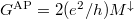
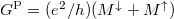
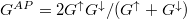
\frac{\Delta G}{G^\mathrm{P}}=\frac{M^\uparrow-M^\downarrow}{M^\uparrow+M^\downarrow}=P_c.
\end{equation}
This simplified model corresponds to the perfectly ballistic limit, where no
backscatterings are considered inside the quantum wire.
. With this notation the relative change of
the conductance turns out to be equal to the current spin polarization
characteristic to the ferromagnetic metal applied,
\begin{equation}
\frac{\Delta G}{G^\mathrm{P}}=\frac{M^\uparrow-M^\downarrow}{M^\uparrow+M^\downarrow}=P_c.
\end{equation}
This simplified model corresponds to the perfectly ballistic limit, where no
backscatterings are considered inside the quantum wire.
In a more realistic model the scattering inside the nanostructure should also be
considered. If the structure is smaller than the phase diffusion length,
 the scattering in the two layers are added coherently, and accordingly
the total resistance relies on the fine details of quantum interference
phenomena.
the scattering in the two layers are added coherently, and accordingly
the total resistance relies on the fine details of quantum interference
phenomena.
\begin{figure} [!h]
\centering
\includegraphics[width=\columnwidth]{fig10.eps}
\caption{\it Resistive model of the GMR effect. The two magnetic layers are
separated by an incoherent nonmagnetic region. The top panel demonstrates the
parallel alignment of the magnetic layers (both layers have
magnetization direction), whereas the bottom panel demonstrates the
antiparallel alignment (the left layer has and the right layer has
magnetization direction).  and
and  denote
the conductance of a layer for electrons with majority and minority spin
direction, respectively.}
\label{GMR2}
\end{figure}
denote
the conductance of a layer for electrons with majority and minority spin
direction, respectively.}
\label{GMR2}
\end{figure}
For even larger junctions, where phase coherence between the two magnetic layers
is already lost ( ), but the spin information is still preserved
(), the two scattering regions are connected \emph{incoherently}
(Fig.~\ref{GMR2}), and accordingly their resistances are simply summed to get
the total resistance.\cite{note1} In this limit the magnetoresistance of the
spin valve structure is also easily calculated. To compare with the previous
ballistic model we calculate with conductances: the conductance for majority
spin states is , whereas for minority spins it is .
For antiparallel oriented magnetic layers the total conductance is
), but the spin information is still preserved
(), the two scattering regions are connected \emph{incoherently}
(Fig.~\ref{GMR2}), and accordingly their resistances are simply summed to get
the total resistance.\cite{note1} In this limit the magnetoresistance of the
spin valve structure is also easily calculated. To compare with the previous
ballistic model we calculate with conductances: the conductance for majority
spin states is , whereas for minority spins it is .
For antiparallel oriented magnetic layers the total conductance is
 , whereas for
parallel oriented layers it is
, whereas for
parallel oriented layers it is 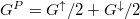 . From these
equations
\begin{equation}
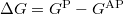
\frac{\Delta G}{G^\mathrm{P}}=\left(\frac{G^\uparrow-G^\downarrow}{G^\uparrow+G^\downarrow}\right)^2=P_c^2
\end{equation}
follows. Note, that this model is equivalent with the common resistor model of the GMR phenomenon.\cite{0022-3727-35-18-201}
. From these
equations
\begin{equation}
\frac{\Delta G}{G^\mathrm{P}}=\left(\frac{G^\uparrow-G^\downarrow}{G^\uparrow+G^\downarrow}\right)^2=P_c^2
\end{equation}
follows. Note, that this model is equivalent with the common resistor model of the GMR phenomenon.\cite{0022-3727-35-18-201}
Both of the above simple models show that  is positive, i.e. the
parallel orientation has higher conductance than the antiparallel one. Depending
on the model, the relative conductance change ranges between
is positive, i.e. the
parallel orientation has higher conductance than the antiparallel one. Depending
on the model, the relative conductance change ranges between  and
and  which indicates that a more complicated model based on the coherent
superposition of two scattering regions would also give a result between the
above two extreme limits. These considerations show that for typical values of
which indicates that a more complicated model based on the coherent
superposition of two scattering regions would also give a result between the
above two extreme limits. These considerations show that for typical values of
 , the relative amplitude of the GMR effect is expected to be
significant regardless of the details of the model. Note, however, that this
is only valid if the spin information is fully preserved in the spacer layer. As
the separation of the magnetic layers becomes larger than the spin diffusion length the GMR
effect exponentially decays.\cite{PhysRevB.48.7099,0953-8984-19-18-183201}
, the relative amplitude of the GMR effect is expected to be
significant regardless of the details of the model. Note, however, that this
is only valid if the spin information is fully preserved in the spacer layer. As
the separation of the magnetic layers becomes larger than the spin diffusion length the GMR
effect exponentially decays.\cite{PhysRevB.48.7099,0953-8984-19-18-183201}
The magnetic layers of a spin valve are decoupled by paramagnetic spacer, and this allows switching between parallel and antiparallel alignments. As the relative alignment depends on the external magnetic field, the GMR effect can be used for magnetic sensing. For this purpose the orientation of one layer is pinned by growing it on top of an antiferromagnet, while the unpinned free layer can rotate even under the influence of a weak magnetic field. Spin valves are extensively applied as the read head of hard disks, which utilizes the fast and reliable reading of the magnetic information by an electric signal.
The spin valve structure can also be used to store magnetic information. This type of non-volatile memory consists of a large number of spin valves, each of them being addressed separately in a crossbar wire architecture. The orientation of the free layer defines bit ``0 and bit ``1, which can be changed by the stray field of the nearby crossing wires. The information written in this way is red out by the GMR effect. However, the areal density of this type of magnetoresistive random access memories (MRAM) is limited by the length scale of the slowly decreasing stray fields.
In the most advanced novel MRAMs no external field (and extra wiring) is required to write information in a spin valve memory element. In these devices the orientation of the free layer is manipulated by high density spin polarized currents, while the magnetic information is obtained by low current GMR measurements. The writing is based on the spin-flip electron scattering processes occurring in the free layer, which exert a torque on the magnetization. Even though such spin-flips are rare events (the spin diffusion length is much larger than the characteristic size of the nanodomain), at current densities of about \(10^9 -10^{10}\, \textrm{A/cm}^2\), the induced torque becomes large enough to reverse the magnetization. The details of the spin transfer torque phenomenon are reviewed in Ref.~\cite{Ralph20081190}. Here we just point out the importance of the strongly non-equilibrium state of this nanoscale device: while the above current densities would lead to melting in any macroscopic metal, in this device the length scales which determine its transparency (i.e. its resistance) are well below the inelastic mean free path, and as a consequence the Joule heat is produced outside the device, in a much larger volume. In spite of the huge current densities, the nanoscale electronics defines appropriate signal levels for practical applications (below \(100\,\mu\)A, and around \(1\,\)V). Finally it is to be noted that the spin transfer torque magnetoresistive random access memory (STT-MRAM) is one of the most promising candidate for future spintronic applications.
\section{Conclusions}
Nanoscale phenomena of spin related transport were discussed both theoretically and experimentally. Based on the spin dependent band structure of a magnetic metal, we discussed the propagation of electrons in the ballistic and diffusive limits, and by applying the Landauer formalism, we supplied a \emph{nanoscopic} background for the conventional expression of the current spin polarization. As the most direct experimental method for spin polarization measurements, the Andreev reflection spectroscopy was introduced, and experimental results on Fe and Co were shown. The analysis demonstrated the reliability of measurements carried out in the ballistic limit. The method was also extended for the determination of the spin diffusion length, one of the most important parameters of metals in spintronic applications. The operation of spin valves was described in terms of the Landauer formalism and the magnitude of the GMR effect was determined in the coherent ballistic and the incoherent diffusive limits. Finally a short overview on spin valve applications was given.