Electron transport in nanowires: Landauer formula, conductance quantization
Tartalomjegyzék |
Characteristic length scales
The conduction properties of a nanoscale object differ from the familiar features on the macroscopic scale.
The resistance of a macroscopic wire is well described using Ohm’s law: the current density ( ) equals to the conductivity (
 ) multiplied by the electric field (
 ); the conductance (
 ) is proportional to the cross-section of the wire (
 ) and inversely proportional to its length (
 ):
):
![\[\vec{j}=\sigma \cdot \vec{E}, \ \ \ G=R^{-1}=\frac{A\cdot \sigma}{L}\]](/images/math/7/b/c/7bc09554c31016e9d495c03164518ac1.png)
Ohm’s law is easily explained by the Drude model of electric conduction: the electrons travel in the crystal lattice gaining  momentum and then losing it by scattering into a random direction. The time elapsed between two scattering events is called the momentum relaxation time and is denoted by
  . The momentum gained by the electrons in time is:
![\[p_\mathrm{drift}=m\cdot v_\mathrm{drift}=eE\tau_\text{m}.\]](/images/math/d/e/a/dea37f6b81839d7d09148a38ae1948f4.png)
According to this, the current density and the conductivity in case of electron density  :
:
![\[\vec{j}=n\cdot e\cdot v_\mathrm{drift}\ \ \ \rightarrow \ \ \ \sigma=\frac{ne^2\tau_\text{m}}{m}.\]](/images/math/a/7/c/a7cf74f960f47af7c9ac7fc6ae2c818b.png)
Between two scattering events -- in time  -- electrons travel a distance
  , where
  is the Fermi velocity. This distance is called the momentum relaxation length. The Drude model loses its meaning if the characteristic size () of the wire in question is less than the momentum relaxation length characterizing the scale of the scatterings. Based on this we can differentiate between diffusive and ballistic wires. In the diffusive case (
 ) the electrons scatter many times before they get from one electrode into the other (figure 1/a), while in the ballistic case (
 ) the electrons scatter don't scatter inside the wire, only on its walls (figure 1/b).
 |
 |
| Figure 1/a. Diffusive wire | Figure 1/b. Ballistic wire |
The length dependence of the resistance clearly demonstrates the difference between the two limiting cases: while the resistance of a diffusive wire increases by lengthening the wire, the electrons that get in a ballistic wire can travel through it without scattering back, i.e. that the resistance does not depend on the length of the wire.
Taking into account the wave nature of electrons it is worth to investigate whether the phase information of electrons is conserved or not on the size-scale of the examined system. If the size of the sample is smaller than the  phase-relaxation length, then the conduction properties show interesting interference phenomena that can’t be seen on the macroscopic scale. We cover these phenomena in chapter interference and decoherence in nanostructures.
Another interesting question is whether the spin information of electrons is conserved in the nanostructure under investigation. In nanostructures that are smaller than the so-called spin diffusion length ( ) and contain magnetically ordered regions interesting spintronic phenomena can be observed.
Further interesting phenomena occur if the cross-section of the wire becomes comparable to the Fermi wavelength of electrons:  . We explain this below.
Resistance of quantum wires
Let’s consider the properties of nanowires comparable with the wavelength of electrons using a simple model: we connect two electron reservoirs with a 2-dimensional ideal quantum wire with parallel walls, in which the electrons travel without scattering (figure 2.).
 |
| Figure 2. Ideal quantum wire |
Using hard wall boundary condition (i.e. the enclosing potential is zero inside and infinite outside of the wire) the wavefunction of the electrons:
![\[\Psi_{n,k}(x,y)=e^{ikx}\cdot \sin\left(\frac{n \pi y}{W} \right),\]](/images/math/c/b/b/cbb631029abef03f779de5d448cf7b17.png)
that is, in the longitudinal direction we get plane wave propagation, while in the transversal direction standing waves. According to this the energy of the electrons:
![\[\varepsilon_n(k)=\frac{\hbar^2k^2}{2 m} + \frac{\pi^2 \hbar^2}{2 m W^2}\cdot n^2,\]](/images/math/c/7/7/c772508502b24caf1faa4c68c5109a51.png)
where  is the wavenumber belonging to the plane wave propagation along the
  -direction and describes the quantised transverse modes (standing waves along the
  -direction). This expression for the energy corresponds to the one-dimensional energy dispersion relation offset by the transverse mode energies as depicted in the figure. Reasonably, current can only flow through those modes (the so-called conduction channels) that have transverse mode energies smaller than the Fermi energy of the electrodes that is, the dispersion relation intersects with the Fermi level. The modes that satisfy this criterion, are called open conduction channels and the number of open conduction channel is denoted by
  .
.
 |
 |
| 3/a. ábra. Dispersion relation in an ideal quantum wire | 3/b. ábra. Dispersion relation when a bias is applied to the sample |
If we turn on  bias between the two electron reservoirs, the electron states of the nanowire will be filled as represented in figure 3/b. The states with positive values originate from the left electrode, so these are filled to energies
  higher than the states coming from the right electrode with negative values. Only the states with positive and in the region between chemical potentials
  and
and  contribute to the current transport, as below the chemical potential both the positive and negative propagating states are filled, so the total current becomes zero.
For a given conduction channel the velocity of the electrons and the density of states are as follows:
![\[v_n=\frac{1}{\hbar}\frac{\partial \varepsilon_n(k)}{\partial k},\ \ \ \ g_n=\frac{L}{2\pi}\left(\frac{\partial \varepsilon_n(k)}{\partial k}\right)^{-1}.\]](/images/math/f/4/f/f4f7ceadc88e3403d53b0023da1ad7c4.png)
The electron density in the range is calculated as:  . To calculate the total current flowing through the wire we multiply the electron charge, the velocity and the electron density then sum these up for the individual conduction channels:
![\[I=2\sum_{n=1}^{M}e v_n n_n =\frac{2e^2}{h}MV,\]](/images/math/6/1/c/61ce1c2052a80ff9f33efa0b2b800ba5.png)
where the multiplier 2 corresponds to the spin degeneracy. Since the derivative of the energy dispersion in the product of the velocity and the electron density cancels, the conductance of the quantum wire is simply the integer multiple of the conductance quantum  . It’s worth to note that momentum is conserved in the -direction due to the longitudinal translation invariance, which prohibits the scattering between conduction channels, as it would change the wavenumber so we really can treat the current contribution of the individual conduction channels independently.
The above calculation was derived from the assumption that occupied states are only to be found below the chemical potential  of the electrodes that is, the temperature is zero. At finite temperature, we can find both occupied and unoccupied states in the
  wide range around the chemical potential. The possibility of a state being occupied is described by the Fermi function:
![\[f(\varepsilon)=\frac{1}{e^{\frac{\varepsilon -\mu}{k_{\text{B}}T}}+1}.\]](/images/math/6/c/3/6c3faca094e66816c7e7afcf3d3a8f79.png)
Inside the quantum wire the electron states originating from the left electrode ( ) are occupied according to
  , the occupation number function of electrode 1, while the electron states from the right electrode (
 ) according to
  the occupation number function of electrode 2. Here and are Fermi functions offset with energy relative to each other. This description also presumes the electron reservoirs to be perfect: the electrons that enter the electrode from the quantum wire can scatter back into the quantum wire only after thermalisation, so the electrons leaving the electrode truly follow the energy distribution that corresponds to the Fermi function of the given electrode.
As a consequence of the arguments above, the current flowing in the wire at finite temperature into the positive and the negative direction respectively:
the occupation number function of electrode 2. Here and are Fermi functions offset with energy relative to each other. This description also presumes the electron reservoirs to be perfect: the electrons that enter the electrode from the quantum wire can scatter back into the quantum wire only after thermalisation, so the electrons leaving the electrode truly follow the energy distribution that corresponds to the Fermi function of the given electrode.
As a consequence of the arguments above, the current flowing in the wire at finite temperature into the positive and the negative direction respectively:
![\[I^+=\frac{2 e}{L} \sum \limits_{k>0} v_k f_1(\varepsilon_k) = 2e \int \frac{\mathrm{d}k}{2 \pi}\frac{\partial \varepsilon_k}{\hbar \partial k} f_1(\varepsilon_k) = \frac{2 e}{h}\int \mathrm{d} \varepsilon f_1(\varepsilon),\]](/images/math/3/1/c/31c4678e29410e7fa637f9687cb858a1.png)
![\[I^-=\frac{2 e}{L} \sum \limits_{k<0} v_k f_2(\varepsilon_k) = \frac{2 e}{h}\int \mathrm{d} \varepsilon f_2(\varepsilon),\]](/images/math/e/2/f/e2f6fb8f6d0d0eadf5b25d606c80db97.png)
i.e. the total current is:
![\[I=I^+-I^-=\frac{2 e}{h} \int \mathrm{d} \varepsilon (f_1(\varepsilon)-f_2(\varepsilon))=\frac{2 e}{h}e V.\]](/images/math/e/8/0/e80de55ed30db22f813dd9ffdbc36397.png)
The integral  equals eV at any finite temperature, which infers the conductance of a single-channel ideal quantum wire to be the conductance quantum,
  at arbitrary temperature, which corresponds to a resistance of
  .
.
Landauer-formula
Most tekintsük azt az egyszerű modellt, amikor egy egycsatornás, ideális kvantumvezeték közepén egy szórócentrum található, melyen  valószínűséggel jutnak át az elektronok. Ebben az esetben az elektródák felől a szórócentrum felé haladó állapotok továbbra is a megfelelő elektródából származnak, és ennek az eloszlásfüggvényét követik (lásd a 4. ábrán a
  és
és  áramkomponenseket). A szórócentrumtól az elektródák felé haladó állapotok viszont kevertek, pl. a
  áramjáruléknál egyaránt figyelembe kell venni az 1-es elektródából induló és a szórócentrumon reflektálódó, illetve a 2-es elektródából induló és a szórócentrumon transzmittálódó elektronokat.
 |
| 4. ábra. Egycsatornás kvantumvezeték átmeneti valószínűségű szórócentrummal
|
Zérus hőmérsékleten csak a kémiai potenciál alatti állapotok származhatnak mindkét elektródából, azonban az  állapotok teljes árama értelemszerűen zérust ad, hiszen ez annak felel meg, mintha zérus feszültséget kapcsoltunk volna a rendszerre. Így a véges áramért továbbra is
  állapotok felelnek, melyek csak az 1-es elektródából származhatnak. Így a teljes áram könnyen számolható például a szórócentrum és a 2-es elektróda közötti vezetékdarabban. Itt a
energiasávban levő elektronok
állapotok felelnek, melyek csak az 1-es elektródából származhatnak. Így a teljes áram könnyen számolható például a szórócentrum és a 2-es elektróda közötti vezetékdarabban. Itt a
energiasávban levő elektronok  esetén a korábbiak alapján
  áramot adnának, ami
  esetén értelemszerűen a transzmittálódó elektronok hányadával skálázódik, azaz
  . Így egy egycsatornás, transzmisszós valószínűségű szórócentrumot tartalmazó nanovezeték vezetőképessége:
![\[G=\frac{2e^2}{h}\mathcal{T} .\]](/images/math/3/c/3/3c33c14c13478a7d5031d6b5b51ced23.png)
Vizsgáljuk meg, hogy ez az eredmény érvényes-e véges hőmérsékleten is. A és áramkomponensek kizárólag az 1-es illetve a 2-es elektródából származnak, így a korábbiak alapján egy  energiatartományban az áramjárulékuk:
![\[\mathrm{d}I_1^+(\varepsilon)=\frac{2 e}{h}\cdot f_1(\varepsilon)\mathrm{d}\varepsilon,\;\; \mathrm{d}I_2^-(\varepsilon)=\frac{2 e}{h}\cdot f_2(\varepsilon)\mathrm{d}\varepsilon.\]](/images/math/e/9/8/e983f21ad16c4ed34dc48057d58842ce.png)
Ha az áramot a szórócentrum és az 1-es elektróda közötti vezetékdarabon akarjuk kiértékelni, akkor szükségünk van a áramjárulékra is, mely valószínűséggel a 2-es elektródából bejövő módus transzmissziójából,  valószínűséggel pedig pedig a az 1-es elektródából bejövő módus reflexiójából származik:
![\[\mathrm{d}I_1^-(\varepsilon)=\mathrm{d}I_1^+(\varepsilon)\cdot (1-\mathcal{T}) + \mathrm{d}I_2^-(\varepsilon)\cdot \mathcal{T},\]](/images/math/1/c/a/1ca0063385d01527198c7d015ff1c0a9.png)
így a negatív és pozitív irányba haladó áramkomponensek együttes járuléka:
![\[\mathrm{d}I_1=\mathrm{d}I_1^+ - \mathrm{d}I_1^- = \frac{2 e}{h} \cdot \mathcal{T} \cdot [f_1(\varepsilon)-f_2(\varepsilon)]\mathrm{d}\epsilon.\]](/images/math/f/3/9/f39db877ac18b4c6636656330ee65181.png)
A teljes áramot integrálással kapjuk meg:
![\[I=\frac{2 e}{h} \cdot \int \mathcal{T}\cdot [f_1(\varepsilon)-f_2(\varepsilon)]\mathrm{d}\varepsilon.\]](/images/math/f/c/b/fcb985a47ca9ef664771724359b3c658.png)
A két Fermi-függvény különbsége a és kémiai potenciálok közötti energiatartományban, illetve a két kémiai potenciál körüli  energiatartományban különbözik zérustól. Feltételezve hogy ebben a tartományban a transzmisszós valószínűség energiafüggetlen, és kihasználva a
  azonosságot a vezetőképességre véges hőmérsékleten is a
![\[G=\frac{2 e^2}{h}\cdot \mathcal{T}\]](/images/math/3/9/c/39c19c41cf54b36e17aafebf82ee4a19.png)
eredményt kapjuk. Ha a transzmissziós valószínűség nem tekinthető energiafüggetlennek, akkor -t a releváns energiatartományra vett átlagos transzmissziós valószínűségnek kell tekinteni.
 |
5. ábra. Többcsatornás kvantumvezeték leírása  transzmissziós mátrixszal transzmissziós mátrixszal
|
Több vezetési csatorna esetén a szórócentrum hatását egy komplex transzmissziós mátrixszal () írhatjuk le, mely a bal oldalon az egyes csatornákban bejövő, azaz az elektródától a szórócentrum felé haladó illetve a jobb oldalon kimenő, azaz a szórócentrumtól az elektróda felé haladó módusok között teremt kapcsolatot:
![\[\left| \mathrm{ki} \right>_2=\hat{t} \left| \mathrm{be} \right>_1.\]](/images/math/3/1/5/3157e2b71d142f8d8906ed5935cf03e9.png)
Megmutatható, hogy a vezetőképesség ebben az esetben
![\[G = \frac{2 e^2}{h} \mathrm{Tr}(\hat{t}^\dagger \hat{t})\]](/images/math/7/3/1/731d25473a2b91fd02df762b3eef3887.png)
formában írható. A  kifejezést átírhatjuk
  formában, ahol
  a bal oldali i-edik csatornából a jobb oldali j-edik vezetési csatornába történő átszórás valószínűségét adja meg. Ennek megfelelően a vezetőképesség
![\[G = \frac{2 e^2}{h} \sum \limits_{i,j} \mathcal{T}_{j,i}\]](/images/math/d/d/6/dd6a269bd64cb9e81b26fe13d09f4ea4.png)
formában írható. Megfelelő bázisban a probléma diagonalizálható, azaz elérhető hogy a jobb oldali i-edik csatornából csak a bal oldali i-edik csatornába tudjanak szóródni elektronok. Ekkor a rendszer a nyitott vezetési csatornák számának megfelelő  db. egymástól független egydimenziós vezetéknek tekinthető, melyek vezetőképesség-járulékát egyszerűen összegezhetjük:
![\[G = \frac{2 e^2}{h} \sum \limits_{i=1..N} \mathcal{T}_i.\]](/images/math/b/5/d/b5ddacc209168c8bfd3c40d09bd11038.png)
A  operátor sajátértékeinek megfelelő
  transzmissziós együtthatók az i-edik sajátcsatorna transzmissziós valószínűségét adják meg.
Vezetőképesség-kvantálás kvantum-pontkontaktusban
Vegyünk egy olyan kétdimenziós kvantumvezetéket, melyben nincsenek szórócentrumok, a vezeték  szélessége pedig lassan (adiabatikusan) változik a hossztengely mentén (6. ábra alsó panel). A lassan változó szélességnek köszönhetően a vezeték lokálisan mindenütt jól közelíthető egy párhuzamos falú vezetékdarabbal, és a hullámfüggvények leírhatók az adott szélességhez tartozó keresztirányú állóhullámokkal, illetve hosszirányú síkhullám terjedéssel. A 6. ábra felső panele a keresztirányú állóhullámokhoz tartozó energiát ábrázolja a vezeték mentén különböző vezetési csatornákra. Egyértelmű, hogy azon vezetési csatornák tudnak csak átjutni a vezetéken (ú.n. kvantum-pontkontaktuson), melyek keresztirányú energiája a vezeték legkisebb keresztmetszeténél is a Fermi-energia alatt van.
 |
| 6. ábra. Keresztirányú energiák egy adiabatikus kvantum-pontkontaktusban |
A 7. ábra a vezetékben kialakuló diszperziós relációkat mutatja a vezeték két közeli tartományában. A jobb oldali panel egy kicsit keskenyebb vezetékszakaszhoz tartozik mint a bal oldali, így a nagyobb keresztirányú energia miatt a parabolikus diszperziók felfele tolódnak. Mivel a vezeték lokálisan közel transzlációinvariáns, így a hosszirányú impulzus és a hullámszám csak keveset változhat miközben az elektron egy adott tartományból eljut egy másik, közeli tartományba. Egy adott vezetési csatornában hullámszámmal rendelkező állapot a vezeték keskenyedése során csak úgy tud mindig kis impulzusváltozással előre haladni, ha ugyanabban a vezetési csatornában marad (lásd zöld nyíl). Más csatornába történő átszóródás, illetve visszaszóródás esetén jelentősen változna. Kicsit más a helyzet, ha az előrehaladás után az adott csatorna diszperziós relációjának alja a Fermi-energia fölé kerül, azaz az elektron nem tud továbbhaladni. Ebben az esetben az a legkisebb impulzusváltozással járó folyamat, ha nullához közeli de pozitív bejövő -val rendelkező elektron ugyanazon csatorna  állapotába szóródik vissza (piros nyíl).
 |
| 7. ábra. Adiabatikus kvantumvezetékben az elektronok a saját vezetési csatornájukban haladnak előre, illetve ha a csatorna bezáródik, akkor visszaszóródnak |
A fenti érvek alapján elmondható, hogy egy lassan változó szélességű kvantum-pontkontaktusban az összes olyan csatorna, melyhez tartozó keresztirányú energia a legkisebb keresztmetszetben is a Fermi-energia alatt van,  valószínűséggel transzmittálódik (lásd zöld görbék a 6. ábrán), az összes többi csatorna pedig
  valószínűséggel reflektálódik (piros görbék a 6. ábrán), azaz a vezetőképesség a vezetőképesség-kvantum egész számú többszöröse:
![\[G=\frac{2e^2}{h}M,\]](/images/math/a/5/a/a5af2626ce765f8c594e3b30ae49e615.png)
ahol a legkisebb keresztmetszetben elférő keresztirányú módusok száma.
Ez a jelenség kísérletekben is megfigyelhető, elsőként van Wees és szerzőtársai,1 illetve Wharam és szerzőtársai2 demonstrálták a vezetőképesség-kvantálást kétdimenziós elektrongáz-rendszerből kialakított kvantum-pontkontaktusban. A kísérletet sematikusan a 8. ábra szemlélteti. A kétdimenziós elektrongázban két felső kapuelektróda segítségével egy keskeny csatornát alakítunk ki, a csatorna szélessége a kapuelektródákra adott feszültséggel hangolható. Először a kapuelektródák alatt teljesen kiürítjük a kétdimenziós elektrongázt, majd a kapufeszültség változtatásával folyamatosan kinyitjuk a csatornát, és egyre szélesebb pontkontaktust alakítunk ki a két elektróda között. A vezetőképesség eközben lépcsőszerűen változik, először zérusról  -ra nő, majd a vezetési csatornák egyenkénti kinyílásával a vezetőképesség-kvantum egész számú töbszöröseinél látunk platókat.
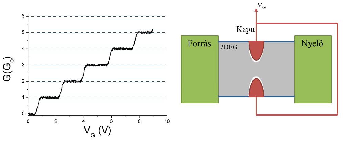 |
| 8. ábra. Vezetőképesség-kvantálás kvantum-pontkontaktusban |
Fontos megjegyezni, hogy egy félvezetőben - így a 8. ábrán szemléltetett kvantum-pontkontaktusban - az elektronok Fermi-hullámhossza párszor tíz nanométer nagyságrendű, így az elektronok nem látják az anyag atomi felépítéséből adódó, tized nanométer nagyságrendű egyenetlenséget, hanem egy sima, közel adiabatikus csatornát látnak. Ezzel szemben fémekben a Fermi-hullámhossz a szomszédos atomok távolságával összemérhető, így egyetlen vagy pár nyitott vezetési csatornával rendelkező pontkontaktust úgy kaphatunk, ha két elektródát mondjuk egyetlen atom köt össze. Ebben az esetben az elektronok a hullámhosszukkal azonos skálán változó, az anyag atomi felépítését tükröző potenciálban mozognak (lásd 9. ábra), melyről nem várjuk hogy adiabatikus legyen, azaz vezetőképesség-kvantálást sem várunk. A kísérletek ezt alá is támasztják,3 a legtöbb fémből készült atomi méretű kontaktusban ugyan csak pár nyitott vezetési csatorna áll rendelkezésre, de az azokhoz tartozó transzmissziós sajátértékek általában tökéletlen transzmissziónak felelnek meg. Atomi mérető kontaktusok viselkedéséről röviden a Nanoszerkezetek előállítási és vizsgálati technikái fejezetben számolunk be.
 |
| 9. ábra. A hullámhossz skáláján változó potenciálban nem várunk vezetőképesség-kvantálást |
Hivatkozások
Fent hivatkozott szakcikkek
Ajánlott könyvek és összefoglaló cikkek
- S. Datta: Electronic Transport in Mesoscopic Systems, Cambridge University Press (1997)
- Thomas Ihn: Semiconducting nanosctructures, OUP Oxford (2010)
- Yuli V. Nazarov, Yaroslav M. Blanter: Quantum Transport: Introduction to Nanoscience, Cambridge University Press (2009)
Ajánlott kurzusok
- Új kísérletek a nanofizikában, Halbritter András és Csonka Szabolcs, BME Fizika Tanszék
- Transzport komplex nanoszerkezetekben, Halbritter András, Csonka Szabolcs, Csontos Miklós, Makk Péter, BME Fizika Tanszék
- Alkalmazott szilárdtestfizika, Mihály György, BME Fizika Tanszék
- Fizika 3, Mihály György, BME Fizika Tanszék (mérnök hallgatóknak)
- Mezoszkopikus rendszerek fizikája, Zaránd Gergely, BME Elméleti Fizika Tanszék
- Mezoszkopikus rendszerek fizikája, Cserti József, ELTE Komplex Rendszerek Fizikája Tanszék