Electron transport in nanowires: Landauer formula, conductance quantization
Tartalomjegyzék |
Characteristic length scales
The conduction properties of a nanoscale object differ from the familiar features on the macroscopic scale.
The resistance of a macroscopic wire is well described using Ohm’s law: the current density ( ) equals to the conductivity (
 ) multiplied by the electric field (
 ); the conductance (
 ) is proportional to the cross-section of the wire (
 ) and inversely proportional to its length (
 ):
):
![\[\vec{j}=\sigma \cdot \vec{E}, \ \ \ G=R^{-1}=\frac{A\cdot \sigma}{L}\]](/images/math/7/b/c/7bc09554c31016e9d495c03164518ac1.png)
Ohm’s law is easily explained by the Drude model of electric conduction: the electrons travel in the crystal lattice gaining  momentum and then losing it by scattering into a random direction. The time elapsed between two scattering events is called the momentum relaxation time and is denoted by
  . The momentum gained by the electrons in time is:
![\[p_\mathrm{drift}=m\cdot v_\mathrm{drift}=eE\tau_\text{m}.\]](/images/math/d/e/a/dea37f6b81839d7d09148a38ae1948f4.png)
According to this, the current density and the conductivity in case of electron density  :
:
![\[\vec{j}=n\cdot e\cdot v_\mathrm{drift}\ \ \ \rightarrow \ \ \ \sigma=\frac{ne^2\tau_\text{m}}{m}.\]](/images/math/a/7/c/a7cf74f960f47af7c9ac7fc6ae2c818b.png)
Between two scattering events -- in time  -- electrons travel a distance
  , where
  is the Fermi velocity. This distance is called the momentum relaxation length. The Drude model loses its meaning if the characteristic size () of the wire in question is less than the momentum relaxation length characterizing the scale of the scatterings. Based on this we can differentiate between diffusive and ballistic wires. In the diffusive case (
 ) the electrons scatter many times before they get from one electrode into the other (figure 1/a.), while in the ballistic case (
 ) the electrons scatter don't scatter inside the wire, only on its walls (figure 1/b.).
 |
 |
| Figure 1/a. Diffusive wire | Figure 1/b. Ballistic wire |
The length dependence of the resistance clearly demonstrates the difference between the two limiting cases: while the resistance of a diffusive wire increases by lengthening the wire, the electrons that get in a ballistic wire can travel through it without scattering back, i.e. that the resistance does not depend on the length of the wire.
Taking into account the wave nature of electrons it is worth to investigate whether the phase information of electrons is conserved or not on the size-scale of the examined system. If the size of the sample is smaller than the  phase-relaxation length, then the conduction properties show interesting interference phenomena that can’t be seen on the macroscopic scale. We cover these phenomena in chapter interference and decoherence in nanostructures.
Another interesting question is whether the spin information of electrons is conserved in the nanostructure under investigation. In nanostructures that are smaller than the so-called spin diffusion length ( ) and contain magnetically ordered regions interesting spintronic phenomena can be observed.
Further interesting phenomena occur if the cross-section of the wire becomes comparable to the Fermi wavelength of electrons:  . We explain this below.
Resistance of quantum wires
Let’s consider the properties of nanowires comparable with the wavelength of electrons using a simple model: we connect two electron reservoirs with a 2-dimensional ideal quantum wire with parallel walls, in which the electrons travel without scattering (figure 2.).
 |
| Figure 2. Ideal quantum wire |
Using hard wall boundary condition (i.e. the enclosing potential is zero inside and infinite outside of the wire) the wavefunction of the electrons:
![\[\Psi_{n,k}(x,y)=e^{ikx}\cdot \sin\left(\frac{n \pi y}{W} \right),\]](/images/math/c/b/b/cbb631029abef03f779de5d448cf7b17.png)
that is, in the longitudinal direction we get plane wave propagation, while in the transversal direction standing waves. According to this the energy of the electrons:
![\[\varepsilon_n(k)=\frac{\hbar^2k^2}{2 m} + \frac{\pi^2 \hbar^2}{2 m W^2}\cdot n^2,\]](/images/math/c/7/7/c772508502b24caf1faa4c68c5109a51.png)
where  is the wavenumber belonging to the plane wave propagation along the
  -direction and describes the quantised transverse modes (standing waves along the
  -direction). This expression for the energy corresponds to the one-dimensional energy dispersion relation offset by the transverse mode energies as depicted in the figure. Reasonably, current can only flow through those modes (the so-called conduction channels) that have transverse mode energies smaller than the Fermi energy of the electrodes that is, the dispersion relation intersects with the Fermi level. The modes that satisfy this criterion, are called open conduction channels and the number of open conduction channel is denoted by
  .
.
 |
 |
| Figure 3/a. Dispersion relation in an ideal quantum wire | Figure 3/b. Dispersion relation when a bias is applied to the sample |
If we turn on  bias between the two electron reservoirs, the electron states of the nanowire will be filled as represented in figure 3/b. The states with positive values originate from the left electrode, so these are filled to energies
  higher than the states coming from the right electrode with negative values. Only the states with positive and in the region between chemical potentials
  and
and  contribute to the current transport, as below the chemical potential both the positive and negative propagating states are filled, so the total current becomes zero.
For a given conduction channel the velocity of the electrons and the density of states are as follows:
![\[v_n=\frac{1}{\hbar}\frac{\partial \varepsilon_n(k)}{\partial k},\ \ \ \ g_n=\frac{L}{2\pi}\left(\frac{\partial \varepsilon_n(k)}{\partial k}\right)^{-1}.\]](/images/math/f/4/f/f4f7ceadc88e3403d53b0023da1ad7c4.png)
The electron density in the range is calculated as: 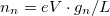 . To calculate the total current flowing through the wire we multiply the electron charge, the velocity and the electron density then sum these up for the individual conduction channels:
![\[I=2\sum_{n=1}^{M}e v_n n_n =\frac{2e^2}{h}MV,\]](/images/math/6/1/c/61ce1c2052a80ff9f33efa0b2b800ba5.png)
where the multiplier 2 corresponds to the spin degeneracy. Since the derivative of the energy dispersion in the product of the velocity and the electron density cancels, the conductance of the quantum wire is simply the integer multiple of the conductance quantum  . It’s worth to note that momentum is conserved in the -direction due to the longitudinal translation invariance, which prohibits the scattering between conduction channels, as it would change the wavenumber so we really can treat the current contribution of the individual conduction channels independently.
The above calculation was derived from the assumption that occupied states are only to be found below the chemical potential  of the electrodes that is, the temperature is zero. At finite temperature, we can find both occupied and unoccupied states in the
  wide range around the chemical potential. The possibility of a state being occupied is described by the Fermi function:
![\[f(\varepsilon)=\frac{1}{e^{\frac{\varepsilon -\mu}{k_{\text{B}}T}}+1}.\]](/images/math/6/c/3/6c3faca094e66816c7e7afcf3d3a8f79.png)
Inside the quantum wire the electron states originating from the left electrode ( ) are occupied according to
  , the occupation number function of electrode 1, while the electron states from the right electrode (
 ) according to
  the occupation number function of electrode 2. Here and are Fermi functions offset with energy relative to each other. This description also presumes the electron reservoirs to be perfect: the electrons that enter the electrode from the quantum wire can scatter back into the quantum wire only after thermalisation, so the electrons leaving the electrode truly follow the energy distribution that corresponds to the Fermi function of the given electrode.
As a consequence of the arguments above, the current flowing in the wire at finite temperature into the positive and the negative direction respectively:
the occupation number function of electrode 2. Here and are Fermi functions offset with energy relative to each other. This description also presumes the electron reservoirs to be perfect: the electrons that enter the electrode from the quantum wire can scatter back into the quantum wire only after thermalisation, so the electrons leaving the electrode truly follow the energy distribution that corresponds to the Fermi function of the given electrode.
As a consequence of the arguments above, the current flowing in the wire at finite temperature into the positive and the negative direction respectively:
![\[I^+=\frac{2 e}{L} \sum \limits_{k>0} v_k f_1(\varepsilon_k) = 2e \int \frac{\mathrm{d}k}{2 \pi}\frac{\partial \varepsilon_k}{\hbar \partial k} f_1(\varepsilon_k) = \frac{2 e}{h}\int \mathrm{d} \varepsilon f_1(\varepsilon),\]](/images/math/3/1/c/31c4678e29410e7fa637f9687cb858a1.png)
![\[I^-=\frac{2 e}{L} \sum \limits_{k<0} v_k f_2(\varepsilon_k) = \frac{2 e}{h}\int \mathrm{d} \varepsilon f_2(\varepsilon),\]](/images/math/e/2/f/e2f6fb8f6d0d0eadf5b25d606c80db97.png)
i.e. the total current is:
![\[I=I^+-I^-=\frac{2 e}{h} \int \mathrm{d} \varepsilon (f_1(\varepsilon)-f_2(\varepsilon))=\frac{2 e}{h}e V.\]](/images/math/e/8/0/e80de55ed30db22f813dd9ffdbc36397.png)
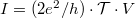
The integral 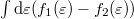 equals eV at any finite temperature, which infers the conductance of a single-channel ideal quantum wire to be the conductance quantum,
  at arbitrary temperature, which corresponds to a resistance of
  .
.
Landauer formalism
Let’s examine the simple model of a single-channel ideal quantum wire with a scattering centre in the middle, which transmits electrons with probability  . In this case, the states travelling from the electrodes in the direction of the scattering region still originate from the corresponding electrode and adhere to its distribution function (see current contributions
  and
and  in figure 4). On the other hand, the states travelling from the scattering region towards the electrodes are mixed, e.g. in case of the
  current contribution both the states backscattered from the scattering region originating from electrode 1 and the states coming from electrode 2 then transmitted by the scattering region.
 |
| Figure 4. Single-channel quantum wire with scattering centre with transmission probability
|
At zero temperature only the states below the chemical potential can come from both of the electrodes, but the total current of the states with  equals to zero because it corresponds to the case where the bias applied to the system is zero. Thus the states with energy
  account for the finite current, which can originate only from electrode 1. So the total current can easily be calculated in the lead section between the scattering centre and electrode 2. Here the electrons in the energy band would give
 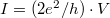 current for
  , which would scale with the number of the transmitted electrons for
  :
:  . So the conductance of a single-channel nanowire with a scattering centre in the middle which has transmission probability
  :
:
![\[G=\frac{2e^2}{h}\mathcal{T}.\]](/images/math/1/7/e/17ef448d62d7bc359f42df27cdb8b65d.png)
Let’s check whether this solution is valid for finite temperatures. The current components and originate solely from electrode 1 or 2, thus their current contributions in the energy range  :
:
![\[\mathrm{d}I_1^+(\varepsilon)=\frac{2 e}{h}\cdot f_1(\varepsilon)\mathrm{d}\varepsilon,\;\; \mathrm{d}I_2^-(\varepsilon)=\frac{2 e}{h}\cdot f_2(\varepsilon)\mathrm{d}\varepsilon.\]](/images/math/e/9/8/e983f21ad16c4ed34dc48057d58842ce.png)
If we want to calculate the current in the lead section between the scattering centre and lead 1, then we also need the current component , which originates with probability from the transmission of the mode coming from electrode 2, or with probability  from the reflection of the mode coming from electrode 1:
![\[\mathrm{d}I_1^-(\varepsilon)=\mathrm{d}I_1^+(\varepsilon)\cdot (1-\mathcal{T}) + \mathrm{d}I_2^-(\varepsilon)\cdot \mathcal{T},\]](/images/math/1/c/a/1ca0063385d01527198c7d015ff1c0a9.png)
so the combined contributions of the currents flowing into the negative and positive directions:
![\[\mathrm{d}I_1=\mathrm{d}I_1^+ - \mathrm{d}I_1^- = \frac{2 e}{h} \cdot \mathcal{T} \cdot [f_1(\varepsilon)-f_2(\varepsilon)]\mathrm{d}\epsilon.\]](/images/math/f/3/9/f39db877ac18b4c6636656330ee65181.png)
We obtain the total current by integration:
![\[I=\frac{2 e}{h} \cdot \int \mathcal{T}\cdot [f_1(\varepsilon)-f_2(\varepsilon)]\mathrm{d}\varepsilon.\]](/images/math/f/c/b/fcb985a47ca9ef664771724359b3c658.png)
The difference of the two Fermi functions differs from zero only in the energy range between the chemical potentials and and the  wide vicinity of the chemical potentials. Assuming that the transmission probability is energy independent, and utilizing the equation
 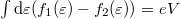 , we get
![\[G=\frac{2 e^2}{h}\cdot \mathcal{T}\]](/images/math/3/9/c/39c19c41cf54b36e17aafebf82ee4a19.png)
for the conductance even for finite temperatures. If the transmission probability cannot be treated energy independently, then has to be considered as the average transmission probability in the relevant energy range.
 |
Figure 5. Description of a multi-channel quantum wire with transmission matrix 
|
In case of more conduction channels the effect of the scattering centre can be described by the complex transmission matrix () (see figure 5.) which connects the incoming modes into the individual channels on the left side propagating from the electrode towards the scattering centre (in figure 5 denoted by  ) and the outgoing modes on the right side propagating from the scattering region in the direction of the electrode (
 in the figure):
![\[\left| \mathrm{out} \right>_2=\hat{t} \left| \mathrm{in} \right>_1.\]](/images/math/4/1/2/412af4551bc707620180107fc587f2c8.png)
One can show that the conductance then is written as:
![\[G = \frac{2 e^2}{h} \mathrm{Tr}(\hat{t}^\dagger \hat{t}).\]](/images/math/5/b/2/5b2aaf381d945f89746eb144dcd28942.png)
One can rewrite  as
as  , where
  gives the probability of scattering from channel
  on the left side into channel
  on the right side. Thus the conductance:
![\[G = \frac{2 e^2}{h} \sum \limits_{i,j} \mathcal{T}_{j,i}.\]](/images/math/0/0/b/00b521e061d3967022701dfad93d6678.png)
Choosing a proper basis one can diagonalise the problem, this way restricting electrons to scatter from channel on the left side solely into channel on the right side. One can then consider the system to consist of N – corresponding to the number of open conduction channels – independent one-dimensional wire and simply sum up their conductance contribution:
![\[G = \frac{2 e^2}{h} \sum \limits_{i=1..N} \mathcal{T}_i.\]](/images/math/b/5/d/b5ddacc209168c8bfd3c40d09bd11038.png)
The  transmission coefficients corresponding to the eigenvalues of the operator
  give us the transmission probability of the th eigenchannel.
Conductance quantisation in a quantum point contact
Now examine a 2-dimensional quantum wire without scattering centres, and let its width decrease slowly (adiabatically) along the longitudinal axis. Thanks to the slowly changing width, the wire approximately consists of parallel-walled wire sections, and the transversal standing waves along with the longitudinal propagating plane waves corresponding to the width of the wire describe the wavefunction. In the upper panel of figure 6 depicts the energy of the transverse modes along the wire for each conduction channel. Obviously, only the channels that have an energy lower than the Fermi energy even in the narrowest portion can get through the wire (the so-called quantum point contact)
 |
| Figure 6. Transverse mode energies in an adiabatic quantum point contact |
Figure 7 shows the dispersion relations in two points inside the wire near to each other. The right one belongs to a somewhat narrower section of the wire, thus the parabolic dispersions are shifted slightly up due to the higher transverse mode energy. As the wire is practically translation invariant, the longitudinal momentum and the wavenumber can only change a little while an electron travels from a given portion to another one near. A state in a given channel with wavenumber can only travel forward with small momentum change inside a wire with decreasing width if it remains in the same conduction channel (see green arrow on figure 7). On the other hand, scattering into another channel or backscattering would change the wavenumber significantly. The situation is different if the dispersion relation of the given channel gets shifted up during the propagation so that it does not cross the Fermi level anymore, prohibiting the electron to go further. In this case, the process that causes the least change in the momentum is that the state with nearly zero but positive scatters back into the state with wavenumber  of the same channel (see red arrow on figure 7).
 |
| Figure 7. In an adiabatic quantumwire electrons propagate forward in their own conduction channel as long as it is open (green arrow). If the channel closes, the electrons are scattered back (red arrow). |
Based on the findings above, all the channels that have energy below the Fermi level even in the narrowest part of the quantum point contact with slowly changing width get transmitted with probability  (see green curves in figure 6), while all other channels get reflected with probability
  (red curves in figure 6). Consequently, the conductance is an integer multiple of the conductance quantum:
![\[G=\frac{2e^2}{h}M,\]](/images/math/a/5/a/a5af2626ce765f8c594e3b30ae49e615.png)
where is the number of transverse modes that fit into the narrowest part of the wire.
This phenomenon is observed in experiments too: The conductance quantisation was first demonstrated by van Wees et al.1 and Wharam et al.2 in a quantum point contact constructed from a two-dimensional electron gas system. The scheme of the experiment is depicted in figure 8. Using two gate electrodes a narrow channel is formed in the two-dimensional electron gas, which has a width tuned by the voltage applied across the gate electrodes. First, the two-dimensional electron gas is totally depleted below the gate electrodes, then the channel is opened changing the applied voltage, and a continuously wider point contact is formed between the two electrodes. In the meantime, the conductance changes steplike: at first, it increases from zero to 2e^2/h, which is followed by other plateaus at integer multiples of the conductance quantum, as a result of conduction channels opening one by one.
 |
| Figure 8. Conductance quantisation in a quantum point contact. Here Kapu means the gate, Forrás and Nyelő mean source and drain respectively. |
It's important to note that in a semiconductor - thus in the quantum point contact in figure 8 - the Fermi wavelength of electrons is on the order of a few ten nanometers such that the electrons don't see the unevenness on a scale of a few tenths nanometer coming from the atomic structure of the material. On the contrary, in metals, the Fermi wavelength is comparable to the distance of neighbouring atoms, thus point contacts with one or a few open channels are formed if the two electrodes are connected by one single atom. In this case, the electrons move in a potential that changes on the scale of the wavelength of electrons and thus reflects the atomic structure of the material which is not assumed to be adiabatic, so no conductance quantisation is expected. This is confirmed by experiments too,3 though only a few conduction channels are available in most of the metallic atomic contacts, their transmission eigenvalues mostly correspond to imperfect transmission. We briefly address the behaviour of atomic size contacts in chapter Construction and study of nanostructures
 |
| Figure 9. In a potential that is changing on the scale of the wavelength of electrons no conductance quantisation is expected. |
Bibliography
Articles referenced above
Recommended books and review articles
- S. Datta: Electronic Transport in Mesoscopic Systems, Cambridge University Press (1997)
- Thomas Ihn: Semiconducting nanosctructures, OUP Oxford (2010)
- Yuli V. Nazarov, Yaroslav M. Blanter: Quantum Transport: Introduction to Nanoscience, Cambridge University Press (2009)
Recommended courses
- Új kísérletek a nanofizikában, Halbritter András és Csonka Szabolcs, BME Fizika Tanszék
- Transzport komplex nanoszerkezetekben, Halbritter András, Csonka Szabolcs, Csontos Miklós, Makk Péter, BME Fizika Tanszék
- Alkalmazott szilárdtestfizika, Mihály György, BME Fizika Tanszék
- Fizika 3, Mihály György, BME Fizika Tanszék (mérnök hallgatóknak)
- Mezoszkopikus rendszerek fizikája, Zaránd Gergely, BME Elméleti Fizika Tanszék
- Mezoszkopikus rendszerek fizikája, Cserti József, ELTE Komplex Rendszerek Fizikája Tanszék