Atomic nanowires (Nobel Prize Physics in Everyday Application – Laboratory Exercise)
Introduction
The idea that matter is made up of atoms dates back to the ancient Greeks. This hypothesis was proven via a series of experiments in the early 20th century, but it was not until 1981 that Gerd Binnig and Heinrich Rohrer built the first scanning tunnelling microscope (STM) able to image atoms on the surface of matter, for which they were awarded the Nobel Prize five years later.
The operation of the scanning tunnelling microscope is based on a special consequence of the wave nature of electrons, which means that current flows between two pieces of metal brought very close to each other, even if they do not touch. This current is called the quantum mechanical tunnelling current, which has the interesting property that it depends very sensitively on the distance between the two metals: if the gap width is reduced by just half an atom-atom distance, the current increases tenfold. This behaviour is demonstrated in Figure 1.
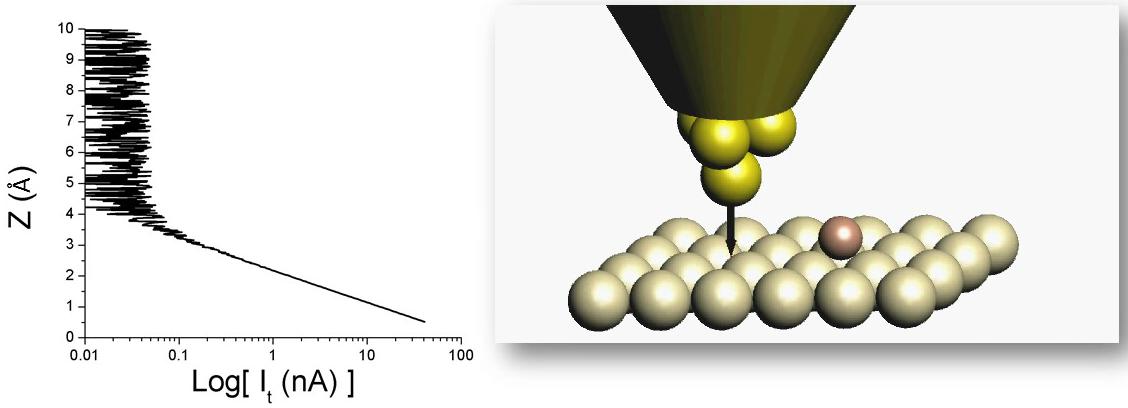 |
Figure 1. A voltage bias is applied between a sharp metallic tip and a metal surface, and the current is measured while the tip is approached to the surface. As long as the tip is far away from the surface, the current is so small that we cannot resolve it with our amperemeter. As the distance between the tip and the surface becomes comparable to the distance between two adjacent atoms, we begin to detect a finite current. The current is plotted on a so-called logarithmic scale, i.e., one step on the Y axis corresponds to a tenfold change in current. The distance of the tip to the surface is given in Angstroms (Å), which correspond to  meters. meters.
Source: András Magyarkuti’s diploma lecture, BME Department of Physics, 2013. |
Even with a not very sharp tip (e.g., a metallic wire cut with scissors), there is an atom on the apex of the tip that is located a little closer to the surface than the other atoms. Because of the sensitive distance dependence, a significant part of the tunnel current will flow through this single atom. By exploiting this, the metal surface can be mapped with atomic resolution by controlling the movement of the tip appropriately. The tip scans the metal surface, while a control circuit is used to move the tip in a direction perpendicular to the surface so that the measured tunnelling current is always constant, i.e., the tip is kept at a nearly constant distance from the sample while scanning its surface (Figure 2). By recording the tip height on a computer, the surface image can be reconstructed. Figure 3 shows an atomic resolution image of a graphite surface taken with a scanning tunnelling microscope.
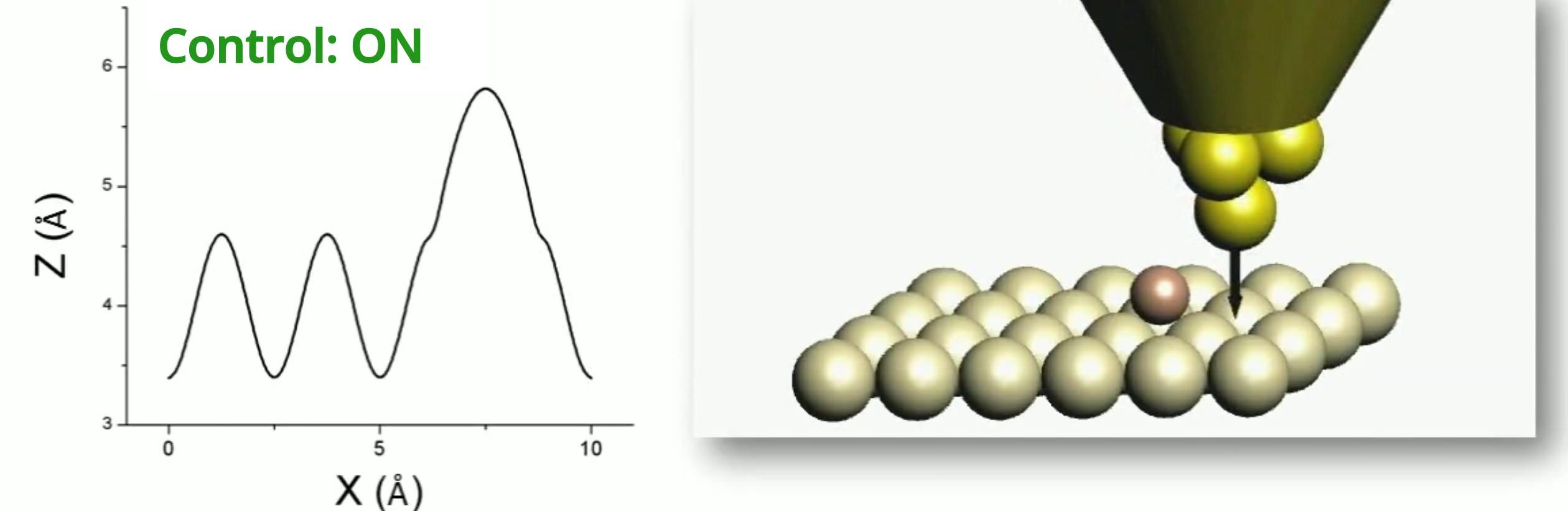 |
| Figure 2. While the tip is moved with constant velocity parallel to the surface, it is positioned in a direction perpendicular to the surface so that the tunneling current, along with the distance between the sample and the tip, remains constant (left side). Based on the movement of the tip, we can reconstruct the image of the surface with atomic resolution (right side).
Source: András Magyarkuti’s diploma lecture, BME Department of Physics, 2013. |
 |
| Figure 3. Atomic resolution image of the surface of a graphite sample.
Source: András Magyarkuti’s diploma thesis, BME Department of Physics, 2013. |
The tip of a scanning tunnelling microscope can be actuated with atomic precision using piezoelectric ceramics. These materials are also used in everyday life, for example in lighters where a piezoelectric prism is suddenly pressed to create high voltage and the resulting spark ignites the flame. With a piezo actuator, the opposite is done: voltage is applied to the piezoelectric crystal, which causes the material to elongate or shorten a little.
A scanning tunnelling microscope is used not only for imaging, but also for manipulating the surface of a sample at the atomic scale: the tip can be used to move individual atoms on the surface. This technique was used to create the circular shape shown in Figure 4, formed by 48 iron atoms on a copper surface. The tunnelling micrograph shows the standing waves of electrons inside the circle.
 |
| Figure 4. Electron standing waves inside a circle of atoms. Source: Wikipedia |
.jpg)
A scanning tunnelling microscope can also be used to create the thinnest nanowires imaginable. If you push the tip of the microscope into the surface and then start to pull it back, you can draw a nanowire between the surface and the tip. As you pull it apart, the nanowire becomes thinner and thinner, and before it breaks apart, there is only a single atom connecting the two sides.
If we measure the conductance (the reciprocal of the resistance,  ) while breaking a nanowire with a diameter of a few atoms, we get the conductance curves (or breaking curves) shown on the left panel of Figure 5: as the tip is lifted, the conductance decreases not continuously but in discrete steps. When we see a flat plateau, the geometry of the junction does not change much, only the atoms move away from each other elastically. But when it jumps, the atoms suddenly rearrange, and after the jump there are fewer atoms connecting the two sides. In the last step before breaking, the current flows through only one atom.
 |
| Figure 5. (a) Conductance curves of atomic-scale gold nanowires recorded during rupture. The rupture events following each other give similar conductance curves, but they are different in the details. (b) From the conductance curves of many breakings, we can plot a conductance histogram, in which the peaks give the conductances of certain atomic configurations that often form. |
The conductance of a single gold atom is close to a universal constant, called the conductance quantum, defined by the electron charge ( ) and Planck's constant (
 ):
):  . This conductance is equivalent to about
  resistance.
After the breaking event, if the two electrodes are pressed together, the atoms on the broken surfaces recombine, so that the breaking of the nanojunction can be repeated. From the conductance curves recorded over thousands of breaking events, a histogram can be constructed, showing peaks at the conductance values of atomic arrangements that occur frequently. The first peak appears at the conductance quantum, at the conductance of a single-atom contact (Figure 5, right).
In gold nanowires, we also encounter another interesting phenomenon. Measuring the length of the last conduction plateau before breaking, we often obtain a length that is significantly longer than we would expect from the size of a single atom. It can be shown that when a single-atom gold contact is further pulled apart, it does not always break apart, but one can pull an atomic chain of up to seven gold atoms (Figure 6).
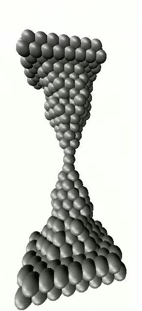 |
| Figure 6. Atomic chain pulling during nanowire rupture (computer simulation). |
In everyday conditions, the resistance of a 7-metre-long wire is exactly seven times that of a one-metre piece of wire. On the atomic scale, however, the behaviour is completely different. The resistance of a seven-atom gold chain is exactly the same as that of a three-atom chain, or a single-atom contact, because once the electrons enter the chain, they pass through to the other side without colliding, regardless of the length of the chain.
Atomic wires can be used to create much smaller electronic devices than current semiconductor transistors, for example in the Department's laboratory we are studying a system where a positive voltage can form a metallic nanowire inside a thin insulator layer, and a negative voltage can break this wire. It is practically a memory device that can store information on the scale of a few nanometres. In addition, atomic scale contacts can be used to study the electrical conduction properties of individual molecules. Once the contact breaks, a narrow nanogap is created to which tiny molecules with the right chemical groups like to bond. Thus, we can even create a bridge made of a single molecule between the two electrodes. The study of nanoscale circuits built from single molecules is the subject of a whole field of nanophysics called molecular electronics. The main goal of this research area is to provide alternatives to current transistors, which consist of hundreds of thousands of atoms. In a laboratory environment, a transistor has already been created with a single fullerene molecule in the active region, amplified by a single electron.
Measurement tasks
During the session, you can experiment with an instrument that is very similar in design to a scanning tunnelling microscope. The principle of the so-called mechanically controllable break junction (MCBJ) arrangement is illustrated in Figure 7. A metal wire is attached by glue or soldered to a flexible plate at two close points. Between the two fixed points, the metal wire is notched by a blade. The flexible plate is supported at both ends and bent in the middle by a stepping motor (rotating an axis) and a piezoelectric actuator. As the plate is bent, the metal wire breaks. With this setup, it is not possible to scan in directions perpendicular to the nanowire, but we can study quantum mechanical tunnelling current, measure the resistance of a single-atom diameter junction, and try out the control technique used in a tunnelling microscope. The advantage of this setup compared to the tunnelling microscope is its superior mechanical stability. It can be calculated that the piezoelectric  elongation results in a displacement in the order of
  between the two sides of the wire, so that any mechanical vibration or displacement due to thermal expansion appears in the elongation of the nanowire reduced by a factor of one hundred. This is the reason why a relatively simple apparatus can be used to carry out experiments on atomic-scaled nanostructures.
 |
| Figure 7. Schematic of the MCBJ setup. |
Assembling the measurement setup
The setup used for the measurement is illustrated in Figure 8. The stepper motor, piezo actuator and metal wire fixed to a flexible plate are mounted in an aluminium frame. The power supply belongs to the motor. The motor and piezo actuator are controlled, and the conductance is measured using a National Instruments myDAQ data acquisition card connected to a computer. The additional circuitry required for the measurement can be assembled on a test panel. The metal wire attached to the leaf spring is shown enlarged in Figure 9.
 |
| Figure 8. Instruments used for the measurement. |
 |
| Figure 9. Metal wire soldered to a flexible plate. |
The TRINAMIC-PD3-013-42 stepper motor is controlled via a four-pole microphone jack mounted on the aluminium frame. Three of the four poles are used to send digital signals from the data acquisition card. One pole is used to turn the motor on and off (ENABLED), the other pole is used to adjust the direction of rotation of the motor (DIRECTION), and a third pole is used to send a short pulse to make the motor take one step, i.e., turn by about 0.1 degrees. The fourth pole is connected to the digital signal ground (DGND). This control cable is used to connect the motor to the data acquisition card. The cable is colour coded: ENABLED - Blue, DIRECTION - Green, STEP - Orange, DGND - Brown.
The pin assignment of the data acquisition card is shown in Figure 10. The signals ENABLED, DIRECTION, STEP, DGND should be connected to the outputs DIO0, DIO1, DIO2 and DGND of the card.
 |
| Figure 10. Channels of the National Instruments myDAQ data acquisition card. |
For fine movement, we use Piezomechanik PSt150/3.5x3.5/20 piezo actuators, which can be operated in the range of -30 V … +150 V, with a total displacement range of 28 μm. The piezo actuator cannot be controlled directly from the myDAQ card, as it would not be able to output high enough current, so an amplifier must be inserted to the circuit. You can set up the amplifier circuit yourself on the test panel using the circuit diagram in Figure 11.
 |
| Figure 11. Circuit diagram of the amplifier used for the piezoelectric actuator. |
The operation of the circuit can be easily understood from the ideal operational amplifier model. The amplifier (marked by a triangle in Figure 11) can be modelled in such a way that the voltage between the "+" and "-" inputs is negligible and both inputs have a huge input resistance, i.e. there is practically no current flowing through these inputs. As a result, the "+" input takes the value of the input voltage,  . Based on the above model, the "-" input also takes the voltage
  . The output of the amplifier is accordingly
 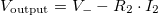 . Since there is no current flowing at the "-" input,
 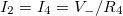 } can be written. Summing up the above, the amplification can be described by the following equation (in case of the circuit shown in Figure 11):
![\[V_\mathrm{output}=V_\mathrm{input}\left(1-\frac{R_2}{R_4}\right).\]](/images/math/a/2/f/a2f98d05f2e9864664531f774a80eaf6.png)
The operational amplifier used is the TL081 type IC, which has the pin assignment shown in Figure 12.
 |
| Figure 12. The pin assignment of the TL081 operational amplifier. |
The amplifier is powered from the +15 V and -15 V outputs of the myDAQ card. The input voltage of the amplifier is controlled from the analog output channel AO1 of the card. Resistances  ,
,  k
k ,
,  ,
,  k should be applied, resulting in 1.27 gain (amplification). Connect the amplifier output to the internal point of the BNC connector of the piezo actuator and the analog ground (AGND) to its external point.
Connect the U labelled connector of the metal wire (see Figure 8) to the AO0 output of the card. Measure current through the I terminal, for which you can also assemble your own amplifier as shown in Figure 13. Based on the above reasoning, the output voltage of the amplifier is 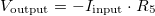 . (This is called a current to voltage converter or current amplifier circuit.) The
  resistance should be
  , and
, and  k as a starting point. Connect the output of the current amplifier to the AI0+ input of the myDAQ, and the AI0- input to ground (AGND).
 |
| Figure 13. Circuit diagram of a current amplifier circuit. |
Measurement of the conductance histogram
Set up the measurement program (see Appendix at the bottom of the page). Apply -100 mV to the sample (this will give a positive voltage at the output of the current amplifier). First set the amplitude of the triangular signal driving the piezo to maximum (10 V amplitude corresponds to a triangular signal between +10 V and -10 V) and set the zero point (OFFSET) to 0 V. Set the current gain (using a feedback resistor of 100 k, this is 100000 V/A, i.e., for  A current, we get 1 V output voltage from the amplifier). First, turn off the trigger and disconnect the wire by moving the motor. When the wire is broken, the measured maximum conductance (determined by the saturation of the amplifier) jumps to 0 in the upper graph of the program. If the position of the motor is adjusted correctly, the piezo actuator driven by the triangular signal will be able to repeatedly break and compress the wire.
Switch on the trigger on so that the top graph shows only the surroundings of a point with a given conductance. This allows us to zoom in on the part of the conductance curves where only a few atoms connect the two sides.
The resolution of the measurement can be improved by reducing the amplitude of the signal driving the piezo. The output of the myDAQ card always realizes the full period of the triangular signal at 100000 discrete points, so the smaller the amplitude of the signal, the closer the adjacent voltage points are to each other. When reducing the amplitude, we can find the piezo voltage range in which we can break and then compress the nanowire by adjusting the OFFSET parameter. It is important to note the amplitude used for each measurement, as this is needed for later calculations.
Take a conductance histogram which shows the peak corresponding to the single-atom contact. Also record individual curves showing the stepwise decrease in conductance. Look for curves in which the last plateau at the quantum conductance is disproportionately long compared to the other plateaus, probably corresponding to atomic chain formation.
Studying the tunneling current
Set the Y axis of the conductance curves to logarithmic. Examine the variation of the tunneling current of the broken contact as a function of piezoelectric voltage, which should be nearly linear on the logarithmic scale (see Figure 1). To resolve the tunneling current, the gain should be increased by one order of magnitude, i.e., the resistance  should be replaced by a resistance of 1 M. The tunneling current should be tested before compression, not after the breaking, because the contact is stretched before breaking, so after the rupture the two electrodes suddenly jump away, and the tunneling current immediately becomes very small.
For this measurement, reducing the amplitude of the piezo drive (to the order of  1 V) and using the trigger are also recommended.
A tenfold change in tunneling current corresponds to approximately m displacement. Calibrate the measuring instrument according to the piezo voltage dependence of the tunneling current. How much displacement between the two sides of the nanowire corresponds to a piezo voltage change of 1 V? On this basis, calculate the factor illustrated in Figure 7, i.e., estimate the reduced amount of piezoelectric displacement in the elongation of the metallic filament.
Stability measurement
During operation of the scanning tunnelling microscope, the control circuit moves the piezo in a direction perpendicular to the sample so that the tunneling current always remains at the desired target value (SETPOINT). If the tunneling current deviates from the target value, the control circuit moves the piezo in such a direction that the difference between the actual tunneling current and the target value, the so-called error signal, is reduced. The control can be characterized by two parameters, one is the so-called  time constant, which characterizes the typical time scale within which the control circuit can respond to a change in the tunneling current. The other parameter is the proportional term
  , which specifies the piezo voltage change that a given magnitude of error term should result in.
Let us simulate the control mechanism of the scanning tunnelling microscope with our measurement setup. The control implemented in the software is not very fast, so we cannot choose a time constant less than 10 ms. Tune the control parameters by setting the target conductance value to  and try to find a setting where the tunneling current deviates as little as possible from the target value. Once this has been achieved, then test the control signal, i.e., observe how the piezo voltage needs to be varied over time to keep the tunneling current constant. Based on the previous calibration, calculate how much the contact would move on a one-minute timescale without control. Also investigate how the system reacts to external excitations, e.g., table knocks, sound effects, etc.
Appendix
Functions of the measurement control program
Figure 14 shows the windows of the measurement control program with different functions.
 |
| Figure 14. Measurement control software. |
The main window is shown on the left, which you can use to record the conductance during a breaking event. When the program starts, you have to enter a file name where the program will save the data. At the beginning of the measurement, set the applied voltage to the sample and the current gain. The parameters of the triangle signal that controls the piezo actuator can be set with the sliders 'Amplitude' and 'Offset'. The measured conductance values are displayed in the upper graph in  units. The data are sampled at a frequency of 100 kHz, i.e., a time of
  ms elapses between two consecutive data points.
Using the Trigger function, you can select the data points of interest from all the measured data. For this, you need to specify a conductance level, a condition (the program starts displaying the data above or below the trigger level), and how many points the program should display before or after the condition is met. The program saves only those data points to the file, which are selected and displayed when the Trigger function is activated. You can also save the data displayed on any other graphs by right-clicking on it, selecting Export from the drop-down menu and clicking Export Data to Clipboard, or selecting Export Data to Excel.
One of the basic tools for evaluating the curves measured during a rupture is the conductance histogram shown on the bottom graph of the main window. This is obtained by dividing the conductance axis of the curves recorded during breaking into equal parts, called bins, and then counting the number of data points falling to each bin. Applying this method to thousands of curves, a histogram similar to Figure 5(b) can be obtained. In the histogram, peaks indicate those conductance values, where plateaus typically appear on the breaking curves.
Pressing the Clear button clears the lower display and restarts the histogram calculation. Pressing the Pause button stops the measurement so that a particular conductance trace can be better examined. Use the tools in the top left corner of the graphs to zoom in on a section of the measured curve.
Use the Controller button to open the control window (centre of Figure 14) and the Motor button to open the window that controls the stepper motor (right side Figure 14).
In the motor control window (right side Figure 14), pressing the Forward or Backward buttons will start the motor to step in the appropriate direction. Make sure that the button labelled Enabled is pressed to enable motor control. In the Delay control, you can set the amount of time in ms units to wait between two steps.
The PIController window (centre of Figure 14) can be used for the control task. It is important that the voltage applied to the sample and the gain of current amplification must be set again. The P and Ti controls are used to set the control parameters. The upper display can show either the conductance or the error signal (the difference between SetPoint and the currently measured conductance). The conductance of the contact is sampled at 1 kHz, but the piezo control output is only updated at 100 Hz frequency. The lower display shows the control signal, i.e., the voltage applied to the piezo.
Help for assembling the circuits
 |
| Figure 15. Piezo amplifier circuit. |
 |
| Figure 16. Current amplifier circuit. |
Instruments used for measurement
- Sample:
 m diameter gold wire soldered to a notched plate
- Sample holder equipped with piezo actuator and stepper motor
- Motor power supply
- NI myDAQ data acquisition card
- Test panel
- TL081 operational amplifier x2
- Resistances:
- 100
- 330 x2
- 2.7 k
- 10 k
- 100 k
- 1 M
- 100
- Cables:
- for the piezo
- for the test panel
- for the motor
- for the sample
- PC with measurement control software