Atomic nanowires (Nobel Prize Physics in Everyday Application – Laboratory Exercise)
Introduction
The idea that matter is made up of atoms dates back to the ancient Greeks. This hypothesis was proven via a series of experiments in the early 20th century, but it was not until 1981 that Gerd Binnig and Heinrich Rohrer built the first scanning tunnelling microscope (STM) able to image atoms on the surface of matter, for which they were awarded the Nobel Prize five years later.
The operation of the scanning tunnelling microscope is based on a special consequence of wave nature of the electrons, which means that current flows between two pieces of metal brought very close to each other, even if they do not touch. This current is called the quantum mechanical tunnelling current, which has the interesting property that it depends very sensitively on the distance between the two metals: if the gap width is reduced by just half an atom-atom distance, the current increases tenfold. This behaviour is demonstrated in Figure 1.
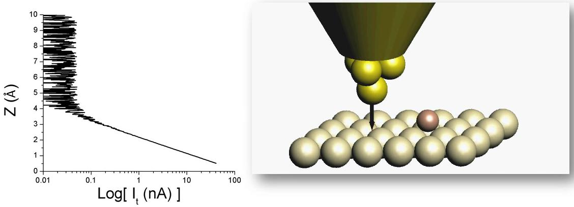 |
Figure 1. A voltage bias is connected between a sharp metallic tip and a metal surface, and the current is measured while the tip is approached to the surface. As long as the tip is far away from the surface, the current is so small that we cannot resolve it with our amperemeter. As the distance between the tip and the surface becomes comparable to the distance between two adjacent atoms, we begin to detect a finite current. The current is plotted on a so-called logarithmic scale, i.e., one step corresponds to a tenfold change in current. The distance of the tip to the surface is given in Angstroms (Å), which correspond to  meters. meters.
Source: András Magyarkuti’s diploma lecture, BME Department of Physics, 2013. |
Even with a not very sharp tip (e.g., a metallic wire cut with scissors), there is an atom on the apex of the tip that is located a little closer to the surface than the other atoms. Because of the sensitive distance dependence, a significant part of the tunnel current will flow through this single atom. By exploiting this, the metal surface can be mapped with atomic resolution by controlling the movement the tip appropriately. The tip scans the metal surface, while a control circuit is used to move the tip in a direction perpendicular to the surface so that the measured tunnel current is always constant, i.e., the tip is kept at a nearly constant distance from the sample while scanning its surface (Figure 2). By recording the tip height on a computer, the surface image can be reconstructed. Figure 3 shows an atomic resolution image of a graphite surface taken with a scanning tunnelling microscope.
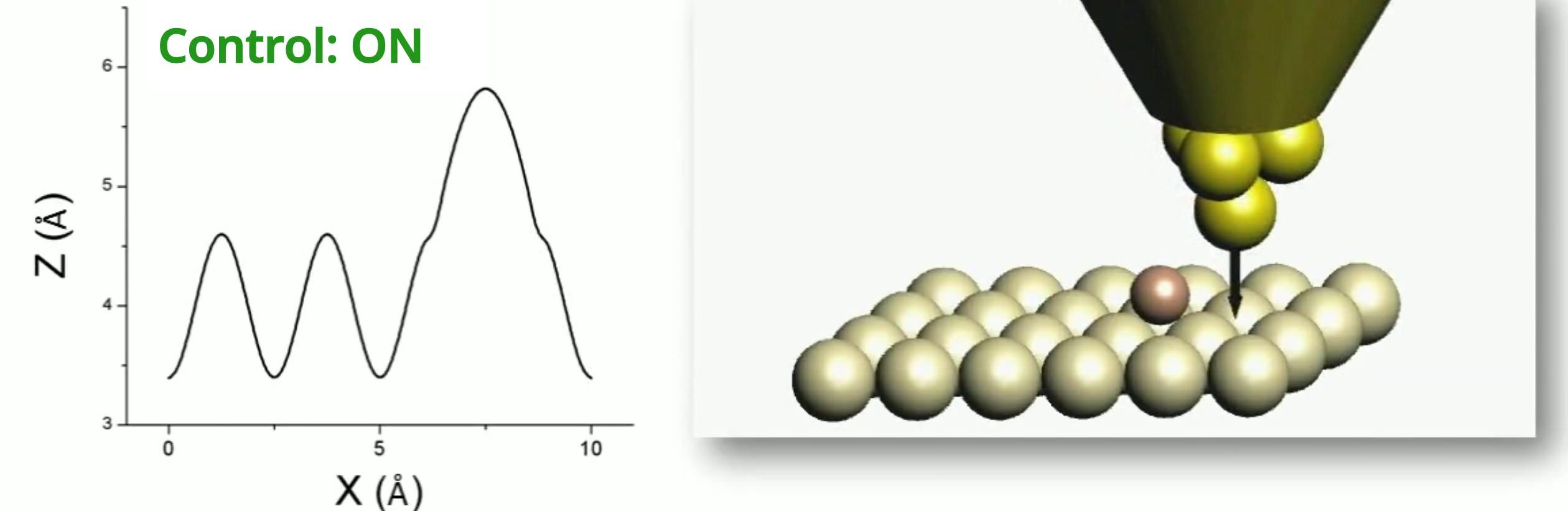 |
| Figure 2. While the tip is moved with constant velocity parallel to the surface, it is positioned in a direction perpendicular to the surface so that the tunnel current, along with the distance between the sample and the tip, remains constant (left side). Based on the movement of the tip, we can reconstruct the image of the surface with atomic resolution (right side).
Source: András Magyarkuti’s diploma lecture, BME Department of Physics, 2013. |
 |
| Figure 3. Atomic resolution image of the surface of a graphite sample. source.
Source: András Magyarkuti’s diploma thesis, BME Department of Physics, 2013. |
The tip of a scanning tunnelling microscope can be actuated with atomic precision using piezoelectric ceramics. These materials are also used in everyday life, for example in lighters where a piezoelectric prism is suddenly pressed to create high voltage and the resulting spark ignites the flame. With a piezo actuator, the opposite is done: an electrical voltage is applied to the piezoelectric crystal, which causes the material to elongate a little.
A scanning tunnelling microscope is used not only for imaging, but also for manipulating the surface of a sample at the atomic scale: the tip can be used to move individual atoms on the surface. This technique was used to create the circular shape shown in Figure 4, formed by 48 iron atoms on a copper surface. The tunnelling micrograph shows the standing waves of electrons inside the circle.
 |
| Figure 4. Electron standing waves inside a circle of atoms. Source: Wikipedia |
.jpg)
A scanning tunnelling microscope can also be used to create the thinnest nanowires imaginable. If you push the tip of the microscope into the surface and then start to pull it back, you can draw a nanowire between the surface and the tip. As you pull it apart, the nanowire becomes thinner and thinner, and before it breaks apart, there is only a single atom connecting the two sides.
If we measure the conductance (the reciprocal of the resistance,  ) while breaking a nanowire with a diameter of a few atoms, we get the conductance curves (or breaking curves) shown on the left panel of Figure 5: as the tip is lifted, the conductance decreases not continuously but in discrete steps. When we see a flat plateau, the geometry of the junction does not change much, only the atoms move away from each other elastically. But when it jumps, the atoms suddenly rearrange, and after the jump there are fewer atoms connecting the two sides. In the last step before breaking, the current flows through only one atom.
 |
| Figure 5. (a) Conductance curves of atomic-scale gold nanowires recorded during rupture. The rupture events following each other give similar conductance curves, but they are different in the details. (b) From the conductance curves of many breakings, we can plot a conductance histogram, in which the peaks give the conductances of certain atomic configurations that often form. |
The conductance of a single gold atom is close to a universal constant, called the conductance quantum, defined by the electron charge ( ) and Planck's constant (
 ):
):  . This conductance is equivalent to about
  resistance.
After the breaking event, if the two electrodes are pressed together, the atoms on the broken surfaces recombine, so that the breaking of the nanojunction can be repeated. From the conductance curves recorded over thousands of breaking events, a histogram can be constructed, showing peaks at the conductance values of atomic arrangements that occur frequently. The first peak appears the conductance quantum, at the conductance of a single-atom contact (Figure 5, right).
In gold nanowires, we also encounter another interesting phenomenon. Measuring the length of the last conduction plateau before breaking, we often obtain a length that is significantly longer than we would expect from the size of a single atom. It can be shown that when a single-atom gold contact is further pulled apart, it does not always break apart, but one can pull an atomic chain of up to seven gold atoms (Figure 6).
 |
| Figure 6. Atomic chain pulling during nanowire rupture (computer simulation). |
In everyday conditions, the resistance of a 7-metre-long wire is exactly seven times that of a one-metre piece of wire. On the atomic scale, however, the behaviour is completely different. The resistance of a seven-atom gold chain is exactly the same as that of a three-atom chain, or a single-atom contact, because once the electrons enter the chain, they pass through to the other side without colliding, regardless of the length of the chain.
Atomic wires can be used to create much smaller electronic devices than current semiconductor transistors, for example in the Department's laboratory we are studying a system where a positive voltage can form a metallic nanowire inside a thin insulator layer, and a negative voltage can break this wire. It is practically a memory device that can store information on the scale of a few nanometres. In addition, atomic scale contacts can be used to study the electrical conduction properties of individual molecules. Once the contact breaks, a narrow nanogap is created to which tiny molecules with the right chemical groups like to bond. Thus, we can even create a bridge made of a single molecule between the two electrodes. The study of nanoscale circuits built from single molecules is the subject of a whole field of nanophysics called molecular electronics. The main goal of this research area is to provide alternatives to current transistors, which consist of hundreds of thousands of atoms. In a laboratory environment, a transistor has already been created with a single fullerene molecule in the active region, amplified by a single electron.
Measurement tasks
During the session, you can experiment with an instrument that is very similar in design to a scanning tunnelling microscope. The principle of the so-called mechanically controllable break junction (MCBJ) arrangement is illustrated in Figure 7. A metal wire is attached by glue or soldered to a flexible plate at two close points. Between the two fixed points, the metal wire is notched by a blade. The flexible plate is supported at both ends and bent in the middle by a stepping motor (rotating an axis) and a piezoelectric actuator. As the plate is bent, the metal wire breaks. With this setup, it is not possible to scan in directions perpendicular to the nanowire, but we can study quantum mechanical tunnelling current, measure the resistance of a single-atom diameter junction, and try out the control technique used in a tunnelling microscope. The advantage of this setup compared to the tunnelling microscope is its superior mechanical stability. It can be calculated that the piezoelectric  elongation results in a displacement in the order of
 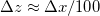 between the two sides of the wire, so that any mechanical vibration or displacement due to thermal expansion appears in the elongation of the nanowire reduced by a factor of one hundred. This is the reason why a relatively simple apparatus can be used to carry out experiments on atomic-scaled nanostructures.
 |
| Figure 7. Schematic of the MCBJ setup. |
Assembling of the measurement setup
The setup used for the measurement is illustrated in Figure 8. The stepper motor, piezo actuator and metal wire fixed to a flexible plate are mounted in an aluminium frame. The power supply belongs to the motor. The motor and piezo actuator are controlled, and the conductance is measured using a National Instruments myDAQ data acquisition card connected to a computer. The additional circuitry required for the measurement can be assembled on a test panel. The metal wire attached to the leaf spring is shown enlarged in Figure 9.
 |
| Figure 8. Instruments used for the measurement. |
 |
| Figure 9. Metal wire soldered to a flexible plate. |
The TRINAMIC-PD3-013-42 stepper motor is controlled via a four-pole microphone jack mounted on the aluminium frame. Three of the four poles are used to send digital signals from the meter card. One pole is used to turn the motor on and off (ENABLED), the other pole is used to adjust the direction of rotation of the motor (DIRECTION), and a third pole is used to send a short pulse to make the motor take one step, i.e., turn by about 0.1 degrees. The fourth pole is connected to the digital signal ground (DGND). This control cable is used to connect the motor to the data acquisition card. The cable is colour coded: ENABLED - Blue, DIRECTION - Green, STEP - Orange, DGND - Brown.
The pin assignment of the data acquisition card is shown in Figure 10. The signals ENABLED, DIRECTION, STEP, DGND are connected to the outputs DIO0, DIO1, DIO2 and DGND of the card.
 |
| 10. ábra. Channels of the National Instruments myDAQ data acquisition card. |
For fine movement, we use Piezomechanik PSt150/3.5x3.5/20 piezo actuators, which can be operated in the range of -30 V … +150 V, with a total displacement range of 28 μm. The piezo actuator cannot be controlled directly from the myDAQ card, as it would not be able to output high enough voltage, so an amplifier must be inserted to the circuit. You can set up the amplifier circuit yourself on the test panel using the circuit diagram in Figure 11.
 |
| Figure 11. Circuit diagram of the amplifier used for the piezoelectric actuator. |
The operation of the circuit can be easily understood from the ideal operational amplifier model. The amplifier (marked by a triangle in Figure 11) can be modelled in such a way that the voltage between the "+" and "-" inputs is negligible and both inputs have a huge input resistance, i.e. there is practically no current flowing through these inputs. As a result, the "+" input takes the value of the input voltage,  V_\mathrm{input}. The output of the amplifier is accordingly
  . Since there is no current flowing at the "-" input,
 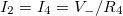 } can be written. Summing up the above, the amplification can be described by the following equation (in case of the circuit shown in Figure 11):
![\[V_\mathrm{output}=V_\mathrm{input}\left(1-\frac{R_2}{R_4}\right).\]](/images/math/a/2/f/a2f98d05f2e9864664531f774a80eaf6.png)
The operational amplifier used is the TL081 type IC, which has the pin assignment shown in Figure 12.
 |
| Figure 12. The pin assignment of the TL081 operational amplifier. |
The amplifier is powered from the +15 V and -15 V outputs of the myDAQ card. The input voltage of the amplifier  is controlled from the analog output channel AO1 of the card. As resistances
  ,
,  k
k ,
,  ,
,  k should be applied, resulting in 1.27 gain (amplification). Connect the amplifier output to the internal point of the BNC connector of the piezo actuator and the analog ground (AGND) to its external point.
A fémszál U jelű csatlakozóját (lásd 8. ábra) kössük a kártya AO0 kimenetére. Egy krokodil csipeszt használva a mintatartó fém keretét földeljük le (AGND). Az I jelű csatlakozón keresztül kell áramot mérnünk, amihez szintén saját erősítőt állítotok össze a 13. ábra kapcsolása alapján. A fenti meggondolások alapján az erősítő kimeneti feszültsége 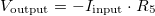 . (Ezt hívjuk áramerősítő kapcsolásnak.) Az
  ellenállás legyen
  Ohm,
Ohm,  -nek pedig kiindulásként kOhm-os ellenállást válasszunk. Az áramerősítő kimenetét csatlakoztassuk a mérőkártya AI0+ bemenetére, az AI0- bemenetet kössük össze az földdel (AGND).
 |
| 13. ábra. Áramerősítő áramkör kapcsolási rajza |
Vezetőképesség-hisztogram mérése
Indítsuk el a mérőprogramot (lásd függelék). A mintára adjunk -100 mV feszültséget (így kapunk az áramerősítő kimenetén pozitív feszültséget). Először állítsuk a piezot meghajtó háromszögjel amplitúdóját maximálisra (a 10V amplitúdó +10 V és -10 V közötti háromszögjelnek felel meg), a nullpontot (OFFSET) pedig állítsuk 0 V-ra. Adjuk meg az áramerősítés értékét (100 kOhm-os visszacsatoló ellenállást alkalmazva ez 100000, azaz  A áramra kapunk 1 V kimenőfeszültséget az erősítőn). Először a triggert kapcsoljuk ki, és a motor mozgatásával szakítsuk el a vezetéket. Mikor elszakad a vezeték, a program felső ábráján a mért maximális vezetőképesség (amit az erősítő telítése határoz meg) 0-ra ugrik. Ha jól állítjuk be a motor pozícióját, akkor a piezora adott háromszögjel ismételten elszakítja és összenyomja a vezetéket.
Kapcsoljuk be a triggert, így a felső ábrán csak egy adott vezetőképességű pont megfelelő szélességű környezetét látjuk. Így kinagyíthatjuk a vezetőképesség-görbék azon szakaszát, ahol már csak pár atom köti össze a két oldalt.
A mérés felbontását javíthatjuk, ha csökkentjük a piezot meghajtó jel amplitúdóját. A kártya kimenete a háromszögjel teljes periódusát mindig 100000 diszkrét pontban valósítja meg, így a piezora kiadott szomszédos feszültségpontok annál közelebb vannak egymáshoz, minél kisebb a jel amplitúdója. Az amplitúdó csökkentésekor az OFFSET állításával találhatjuk meg azt a piezofeszültség-tartományt, melyben el tudjuk szakítani, majd össze tudjuk nyomni a nanovezetéket. Fontos, hogy az alkalmazott amplitúdót minden mérésnél jegyezzük fel, hiszen erre szükség van a későbbi számolásokhoz.
Vegyünk fel egy vezetőképeség-hisztogramot, melyen szépen látszik az egyatomos kontaktusnak megfelelő csúcs. Rögzítsünk egyedi görbéket is, melyeken jól látszik a vezetőképesség lépcsőzetes csökkenése. Keressünk olyan görbéket, melyen az utolsó, vezetőképesség-kvantumnál jelentkező plató aránytalanul hosszú a többi platóhoz képest, ezek valószínűleg atomi láncképződésnek felelnek meg.
Alagútáram vizsgálata
Állítsuk a vezetőképeség-görbék ábrájának Y tengelyét logaritmikus beosztásra. Vizsgáljuk a szétszakadt kontaktus alagútáramának változását a piezofeszültség függvényében, ami a logaritmikus skálán közel egyenes kell hogy legyen (lásd 1. ábra). Ehhez az áramerősítést növeljük meg egy nagyságrenddel, azaz az ellenállást cseréljük le 1 MOhm-os ellenállásra. Az alagútáramot nem a szétszakadás után, hanem az összenyomás előtti tartományban érdemes vizsgálni, hiszen a szétszakadás előtt megnyúlik a kontaktus, így miután elszakad távolra ugrik a két elektróda, így azonnal nagyon kicsivé válik az alagútáram.
Ennél a mérésnél is érdemes a piezomeghajtás amplitudóját lecsökkenteni (1V-os nagyságrendűre), és a triggert használni.
Az alagútáram tízszeres megváltozása hozzávetőlegesen m elmozdulásnak felel meg. Az alagútáram piezofeszültség-függéséből kalibráljátok a mérőeszközt, azaz mondjátok meg, hogy 1 V piezofeszültség-változás a nanovezeték két oldala között mekkora elmozdulásnak felel meg. Ez alapján pontosítsátok a 7. ábrán szemléltetett leosztási tényezőt, azaz becsüljétek meg, hogy a piezomozgató elmozdulása mennyire csökkentett mértékben jelenik meg a fémszál megnyújtásában.
Stabilitás mérése
A pásztázó alagútmikroszkóp működése közben a szabályozó áramkör úgy mozgatja a piezot a mintára merőleges irányban, hogy az alagútáram mindig a kívánt célérték (SETPOINT) maradjon. Ha az alagútáram eltér a célértéktől akkor a szabályozó áramkör olyan irányban mozgatja piezot, hogy az aktuális alagútáram és a célérték közti különbség, az ún. hibajel csökkenjen. A szabályozást két paraméterrel lehet jellemezni, az egyik az ún.  időállandó, ami azt a tipikus időskálát jellemzi, amin belül a szabályozókör válaszolni tud az alagútáram megváltozására. A másik paraméter pedig a
  proporcionális tag, mely azt adja meg, hogy egy adott nagyságú hibajel mekkora piezofeszültség-változást eredményezzen.
Szimuláljuk a mérőberendezésünkön az alagútmikroszkóp szabályozó-mechanizmusát. A szoftverből megvalósított szabályozás nem túl gyors, így időállandónak 10ms-nál kisebb értéket nem választhatunk. 
 vezetőképesség-célértéket beállítva hangoljuk a szabályozás paramétereit, és próbáljunk olyan beállítást találni, melynél az alagútáram minél kevésbé tér el a célértéktől. Ha ezt sikerült megvalósítani, akkor vizsgáljuk a szabályozó jelet, azaz figyeljük, hogy hogyan kell a piezofeszültséget időben változtatni ahhoz, hogy az alagútáram konstans maradjon. A korábbi kalibráció alapján mondjuk meg, hogy egy perces időskálán mennyit mozdulna el a kontaktus szabályozás nélkül. Vizsgáljuk azt is, hogy hogyan reagál a rendszer külső behatásokra, pl. asztal kopogtatása, hanghatás, stb.
Függelék
A mérőprogram funkciói
A 12. ábrán látható a mérésvezérlő program különböző funkciókat ellátó ablakai.
 |
| 12. ábra. Mérésvezérlő szoftver. |
Bal oldalon a fő ablak látható, ezt használhatjuk a szakítási görbék felvételéhez. A program indulásakor meg kell adni egy fájlnevet, ahova a program az adatokat elmenti. A mérés kezdetén állítsuk be a mintára adott feszültséget valamint az áramerősítés mértékét. A piezomozgatót vezérlő háromszögjel paramétereit az 'Amplitude' valamint az 'Offset' feliratú csúszkákkal állíthatjuk. A mért vezetőképesség-értékeket a felső kijelzőn jeleníti meg a program,  mértékegységben. Az adatok mintavételezése 100 kHz frekvenciával történik, vagyis két egymást követő adatpont között
  ms idő telik el.
A Trigger funkciót használva az összes mért adat közül kiválaszthatjuk a számunkra érdekes adatpontokat. Ehhez meg kell adni egy vezetőképességszintet, egy feltételt (a trigger szint felett vagy az alatt kezdje a program az adatok megjelenítését), valamint azt, hogy hány pontot ábrázoljon a program a feltétel teljesülése előtt illetve után. A program csak azokat az adatpontokat menti el az induláskor kiválasztott fájlba, amelyeket a Trigger funkciót bekapcsolva megjelenít a felső kijelzőn. Bármelyik másik kijelzőn megjelenített adatokat is elmenthetjük a következő módon: jobb egérgombbal klikk a kijelzőre, a legördülő menüből válasszuk ki az Export menüpontot, azon belül az Export Data to Clipboard-ra kattintva az adatokat vágólapra helyezhetjük, vagy az Export Data to Excel-re kattintva MS Excel-el elmenthetjük azokat.
A szakítás közben mért görbék kiértékelésének egyik alapvető eszköze a vezetőképesség-hisztogram, amit az alsó kijelző jelenít meg. Ezt úgy kapjuk, ha a szakítási görbék vezetőképesség-tengelyét felosztjuk egyenlő részekre, ún. bin-ekre, majd megszámoljuk, hogy az egyes bin-ekhez hány adatpont tartozik. Ezt elvégezve és összegezve akár több ezer görbére kaphatunk a 5/b. ábrához hasonló hisztogramot. A hisztogramon csúcsok jelzik azokat a vezetőképesség-értékeket, ahol a szakítási görbéken jellemzően platók jelennek meg.
A Clear gombot megnyomva törlődik az alsó kijelző tartalma valamint újraindul a hisztogram számítása. A Pause gombot megnyomva leállíthatjuk a mérést, így jobban megvizsgálható egy adott szakítási görbe. A kijelzők bal felső sarkában található eszközökkel ránagyíthatunk a mért görbék egyes szakaszára.
A Controller gombbal megnyithatjuk a szabályozást végző ablakot (az ábrán középen), valamint a Motor gombbal a léptető motort vezérlő ablakot (az ábra jobb oldalán).
A motort vezérlő ablakban a Forward illetve Backward gombok lenyomásakor a motor a megfelelő irányba kezd el lépegetni. Figyeljünk rá, hogy az Enabled feliratú gomb legyen benyomva, ezzel engedélyezhetjük a motor vezérlését. A Delay vezérlőben állíthatjuk be, hogy két lépés között hány ms ideig várakozzon.
A Controller ablakot a szabályozás feladathoz használhatjuk. Fontos, hogy itt is újra be kell állítani a mintára adott feszültséget valamint az erősítés mértékét. A P illetve Ti vezérlőkben állíthatjuk be a szabályozás paramétereit. A felső kijelző vagy a vezetőképességet vagy a hibajelet (SetPoint és az éppen aktuálisan mért vezetőképesség különbsége) ábrázolhatjuk. A kontaktus vezetőképességét 1 kHz frekvenciával mintavételezi a program, azonban a piezo-t vezérlő kimenetet csak 100 Hz-el frissíti. Az alsó kijelzőn a szabályozó jel, vagyis piezo-ra kapcsolt feszültség látható.
Segítség az áramkörök összeállításához
 |
| 13. ábra. Piezo erősítő kapcsolása. |
 |
| 14. ábra. Áramerősítő kapcsolása. |
A méréshez használt eszközök
- Minta:
 m átmérőjű arany szál középen bevágott lapkára forrasztva
- Mintatartó piezomozgatóval valamint léptetőmotorral felszerelve
- motor tápegység
- NI myDAQ adatgyűjtő kártya
- Próbapanel
- TL081 műveleti erősítő x2
- Elenállások:
- 100 Ohm
- 330 Ohm x2
- 2.7 kOhm
- 10 kOhm
- 100 kOhm
- 1 MOhm
- kábelek:
- piezo-hoz
- próbapanelhez
- motorhoz
- mintához
- PC mérésvezérlő szoftverrel