„Investigation of atomic contacts” változatai közötti eltérés
| 27. sor: | 27. sor: | ||
| − | Let us now approach the formation of the atomic contact from the other side and examine the change in conductivity as the metallic wire is broken. As the wire becomes thinner, we first experience a continuous decrease in conductivity. However, once the diameter of the contact reaches a few atoms, the conductivity can no longer change continuously due to granularity of material on atomic scale. Fig. | + | Let us now approach the formation of the atomic contact from the other side and examine the change in conductivity as the metallic wire is broken. As the wire becomes thinner, we first experience a continuous decrease in conductivity. However, once the diameter of the contact reaches a few atoms, the conductivity can no longer change continuously due to granularity of material on atomic scale. Fig. 3a shows conductivity curves recorded during the breaking of nanocontacts. At first, when the two sides of the contact are pulled apart, the atoms move only elastically relative to one another, while the conductivity changes only moderately (plateau). However, after a certain amount of tension, the atoms rearrange abruptly, resulting in a more favourable configuration with fewer atoms. Atomic rearrangements are reflected by a sudden change in conductance. At the last plateau before the rupture, there is only a single atom connecting the two sides. If the two electrodes are pushed together after rupture, the atoms on the broken surface will be reconnected, so that the breaking of the nanowire can be repeated over and over again (Fig. 3C). Naturally, the conductance curves look different, though similar in nature, for each nanocontact (see Figure 3a for different conductance traces). The characteristic properties of nanocontacts made from a given material can be mapped using statistical methods. A histogram can be plotted from a large number of breaking conductance traces showing how often a given conductivity value was seen during breaking (Fig. 3b). The peaks in the histogram show the conductance of stable, frequently occurring atomic configurations. The first peak of the histogram indicates the conductance of the single-atom contact. It is worth mentioning that in certain materials, e.g. in gold, a single-atom contact does not break apart as a result of pulling, but it can form an atomic chain of up to seven atoms in length, one atom in diameter, as shown in the simulation of Fig. 3C and also by the large peak for the single atom contact in the histogram. |
{| cellpadding="5" cellspacing="0" align="center" | {| cellpadding="5" cellspacing="0" align="center" | ||
| 56. sor: | 56. sor: | ||
To understand the conductance quantum, consider an ideal quantum conductor. (For a more detailed description of all of these, see the [[Transzport_nanovezetékekben:_Landauer-formula,_vezetőképesség-kvantálás|Nanophysics Knowledge Base]].) Imagine a ballistic wire connecting two electrodes without scattering centres, such as the left or right side region on Figure 4 with parallel walls. The motion of electrons in the conductor is described by the Schrödinger equation: transverse quantized modes are formed and electron waves propagate as longitudinal one-dimensional planar waves. | To understand the conductance quantum, consider an ideal quantum conductor. (For a more detailed description of all of these, see the [[Transzport_nanovezetékekben:_Landauer-formula,_vezetőképesség-kvantálás|Nanophysics Knowledge Base]].) Imagine a ballistic wire connecting two electrodes without scattering centres, such as the left or right side region on Figure 4 with parallel walls. The motion of electrons in the conductor is described by the Schrödinger equation: transverse quantized modes are formed and electron waves propagate as longitudinal one-dimensional planar waves. | ||
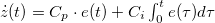
| − | The dispersion relation is: <wlatex>$\epsilon_n(k)=\hbar^2 k^2/2m+E_n$</wlatex>, where <wlatex>$E_n$</wlatex> are the energies of transverse modes. The dispersions belonging to different quantized modes are called the conduction channels. We talk about an open channel if the dispersion relation intersects the chemical potential, but for <wlatex>$E_n>\mu$</wlatex> the channel is closed, that is, no electrons propagate in it. Let us calculate the conductance of the quantum wire for a single conduction channel. Applying voltage to the electrodes shifts the chemical potentials by <wlatex>$\mu_L-\mu_R=eV$</wlatex>-vel, thus states propagating from left to right have higher filling than states from right to left by <wlatex>$eV$</wlatex>. Because of the shift of occupancy, the positive and negative currents are not equal, so in the wire a net current of <wlatex>$I=e\int_{\mu_R}^{\mu_L} n(\epsilon)v(\epsilon)d\epsilon$</wlatex> is present, where <wlatex>$v(\epsilon)=\hbar^{-1} \partial \epsilon/\partial k$</wlatex> is the velocity of electrons, <wlatex>$n(\epsilon)=\rho(\epsilon)/L$</wlatex> is the electron density, with <wlatex>$L$</wlatex> being the length of the wire and <wlatex>$\rho(\epsilon)=\frac{2L}{2\pi\hbar v(\epsilon)}$</wlatex> is the one dimensional density of states. After plugging these in: <wlatex>$I=\frac{2e^2}{h}V$</wlatex>, which corresponds to one channel with a conductance of <wlatex>$G_0 = 2e^2/h$</wlatex> (12906 Ω resistance). The result can be generalized by considering several conducting channels and allowing a finite transmission probability in each channel (Figure 4). The system can be described in a suitable eigenbasis where electrons can only be scattered from the left n-th channel to the right n-th channel. Based on this, the conductance of any nanocontact can be described with the help of the Landauer formula: | + | The dispersion relation is: <wlatex>$\epsilon_n(k)=\hbar^2 k^2/2m+E_n$</wlatex>, where <wlatex>$E_n$</wlatex> are the energies of transverse modes (Fig.5a). The dispersions belonging to different quantized modes are called the conduction channels. We talk about an open channel if the dispersion relation intersects the chemical potential, but for <wlatex>$E_n>\mu$</wlatex> the channel is closed, that is, no electrons propagate in it. Let us calculate the conductance of the quantum wire for a single conduction channel. Applying voltage to the electrodes shifts the chemical potentials by <wlatex>$\mu_L-\mu_R=eV$</wlatex>-vel, thus states propagating from left to right have higher filling than states from right to left by <wlatex>$eV$</wlatex> (Fig. 5b). Because of the shift of occupancy, the positive and negative currents are not equal, so in the wire a net current of <wlatex>$I=e\int_{\mu_R}^{\mu_L} n(\epsilon)v(\epsilon)d\epsilon$</wlatex> is present, where <wlatex>$v(\epsilon)=\hbar^{-1} \partial \epsilon/\partial k$</wlatex> is the velocity of electrons, <wlatex>$n(\epsilon)=\rho(\epsilon)/L$</wlatex> is the electron density, with <wlatex>$L$</wlatex> being the length of the wire and <wlatex>$\rho(\epsilon)=\frac{2L}{2\pi\hbar v(\epsilon)}$</wlatex> is the one dimensional density of states. After plugging these in: <wlatex>$I=\frac{2e^2}{h}V$</wlatex>, which corresponds to one channel with a conductance of <wlatex>$G_0 = 2e^2/h$</wlatex> (12906 Ω resistance). The result can be generalized by considering several conducting channels and allowing a finite transmission probability in each channel (Figure 4). The system can be described in a suitable eigenbasis where electrons can only be scattered from the left n-th channel to the right n-th channel. Based on this, the conductance of any nanocontact can be described with the help of the Landauer formula: |
<wlatex>$$G=\frac{2e^2}{h}\sum\limits_{n}{} T_n,$$</wlatex> | <wlatex>$$G=\frac{2e^2}{h}\sum\limits_{n}{} T_n,$$</wlatex> | ||
A lap 2019. szeptember 18., 11:40-kori változata
The purpose of the measurement is to investigate the transport properties of atomic-sized contacts using the MyDAQ data acquisition card. For this purpose, the conductance curves of nanojunctions are recorded in the last moments before rupture, when only a few atoms connect the two sides. The acquired conductance traces are statistically examined using a conductance histogram.
Introduction: atomic sized contacts
Nowadays, an increasingly important and rapidly growing field of physics research is the study of various nanostructures with a typical width of several hundred - or as we will see - single atoms. Devices of nanometer scale exhibit many astonishing quantum physics processes, as the size of the system becomes comparable to the mean free path of electrons or even to the wavelength of the electrons, and in the case of very small, atomic systems, the atomic quantization of matter must be also taken into account. In addition to studying quantum physical phenomena as part of basic research, nanostructures are playing an increasingly important role in the miniaturization and development of electronic devices. The fabrication of most nanostructures requires a strong technical background based on electron beam lithography, and many quantum physics processes can only be studied at extremely low temperatures (4 K-10 mK). In this measurement we study a nanophysical phenomenon that can be observed at room temperature with a relatively simple measurment system, although the structure under investigation is probably one of the smallest nanostructures: a contact in which two electrodes are connected by a single atom.
A single atom contact is surprisingly easy to create, since at the last moment of breaking a metal wire a single atom connects the two sides. However, the stabilization of the contact is a major challenge, since it is a prerequisite that the mechanical stability of the measuring device is significantly better than a typical atom to atom distance (~ 300 pm). Such conditions can be achieved with a high-stability low-temperature tunnel microscope or with the so-called MCBJ technique (Mechanically Controllable Break Junction technique). The principle of this method is illustrated in Figure 1. The contact is made of a simple metallic wire which is fixed with two adhesive dots on a bending beam. By bending the beam, the attachment points are moving apart so that the metallic wire can be broken. It follows from the mechanical arrangement of the instrument that, when the bending beam is bent in the centre by a gently movable axis, the relative displacement of the electrodes is only 1/100 of the displacement of the axis. If measurements are made at extremely low temperatures in a liquid helium environment and a finely tuneable piezo actuator is used to bend the beam, mechanical stability of up to a few pm can be achieved, which is by an order of magnitude better than what can be achieved using a scanning tunnel microscope.
 |
| Figure 1: The sketch of the MCBJ setup. |
The stability of the system can be tested using the effect of quantum mechanical. If the electrodes are gently moved closer after breaking of the metallic wire, before direct contact occurs, a tunnel current flows between the two sides, the magnitude of which is an exponential function of the electrode spacing. It is calculated that the tunnel current increases approximately tenfold when the electrodes are approached by 100 pm. In low temperature experiments, the exponential distance dependence can be detected through about six orders of magnitude (Figure 2), that is, the conductance increases by about one million times while the electrodes are only approached by 600 µm (two to three times the typical atomic distance). This phenomenon allows for very sensitive detection of changes in the distance between the electrodes. The inset of Figure 2 shows that at a fixed piezo voltage, the electrode spacing changes by only 2 µm in ten minutes, which is about one hundredth of a typical atomic atom spacing. The figure also shows that as the electrodes are approached, a sudden jump is observed at a given point, followed by a conductivity plateau. This creates a direct metallic contact, which in most cases consists of a single atom.
 |
| Figure 2: Tunnel current and mechanical stability test at 4K. |
Let us now approach the formation of the atomic contact from the other side and examine the change in conductivity as the metallic wire is broken. As the wire becomes thinner, we first experience a continuous decrease in conductivity. However, once the diameter of the contact reaches a few atoms, the conductivity can no longer change continuously due to granularity of material on atomic scale. Fig. 3a shows conductivity curves recorded during the breaking of nanocontacts. At first, when the two sides of the contact are pulled apart, the atoms move only elastically relative to one another, while the conductivity changes only moderately (plateau). However, after a certain amount of tension, the atoms rearrange abruptly, resulting in a more favourable configuration with fewer atoms. Atomic rearrangements are reflected by a sudden change in conductance. At the last plateau before the rupture, there is only a single atom connecting the two sides. If the two electrodes are pushed together after rupture, the atoms on the broken surface will be reconnected, so that the breaking of the nanowire can be repeated over and over again (Fig. 3C). Naturally, the conductance curves look different, though similar in nature, for each nanocontact (see Figure 3a for different conductance traces). The characteristic properties of nanocontacts made from a given material can be mapped using statistical methods. A histogram can be plotted from a large number of breaking conductance traces showing how often a given conductivity value was seen during breaking (Fig. 3b). The peaks in the histogram show the conductance of stable, frequently occurring atomic configurations. The first peak of the histogram indicates the conductance of the single-atom contact. It is worth mentioning that in certain materials, e.g. in gold, a single-atom contact does not break apart as a result of pulling, but it can form an atomic chain of up to seven atoms in length, one atom in diameter, as shown in the simulation of Fig. 3C and also by the large peak for the single atom contact in the histogram.
 |
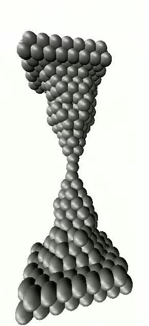 |
| Figure 3a: Conductance traces recorded during the breaking of a gold wire. The subsequent curves are similar in nature, but different in detail. After several breaking cycles the conductance histogram can be calculated and plotted as shown on panel b. The peaks in the histogram give the conductance value of frequently occurring atomic configurations | Figure 3c: Breaking of an atomic wire (computer simualtions). |
Understanding the conduction mechanism of a single atom requires a quantum mechanical approach, since the diameter of the contact is of the same order of magnitude as the wavelength of the electrons. Conductance is through quantized conduction channels whose conductivity must not exceed the quantum conductance unit,  .
.
 |
Figure 4:The conductance properties of atomic contacts can be modeled with two ideal leads separated by a scattering region. The n-th channel on the left is transmitted through the scattering region to the n-th mode on the right with a probability of  . .
|
 |
| Figure 5: (a)Dispersion relation in a nanowire. (b) The occupation in the dispersion relation changes due to the applied bias voltage. |
To understand the conductance quantum, consider an ideal quantum conductor. (For a more detailed description of all of these, see the Nanophysics Knowledge Base.) Imagine a ballistic wire connecting two electrodes without scattering centres, such as the left or right side region on Figure 4 with parallel walls. The motion of electrons in the conductor is described by the Schrödinger equation: transverse quantized modes are formed and electron waves propagate as longitudinal one-dimensional planar waves.
The dispersion relation is:  , where
  are the energies of transverse modes (Fig.5a). The dispersions belonging to different quantized modes are called the conduction channels. We talk about an open channel if the dispersion relation intersects the chemical potential, but for
  the channel is closed, that is, no electrons propagate in it. Let us calculate the conductance of the quantum wire for a single conduction channel. Applying voltage to the electrodes shifts the chemical potentials by
  -vel, thus states propagating from left to right have higher filling than states from right to left by
  (Fig. 5b). Because of the shift of occupancy, the positive and negative currents are not equal, so in the wire a net current of
  is present, where
 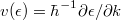 is the velocity of electrons,
  is the electron density, with
  being the length of the wire and
  is the one dimensional density of states. After plugging these in:
  , which corresponds to one channel with a conductance of
  (12906 Ω resistance). The result can be generalized by considering several conducting channels and allowing a finite transmission probability in each channel (Figure 4). The system can be described in a suitable eigenbasis where electrons can only be scattered from the left n-th channel to the right n-th channel. Based on this, the conductance of any nanocontact can be described with the help of the Landauer formula:
![\[G=\frac{2e^2}{h}\sum\limits_{n}{} T_n,\]](/images/math/d/5/6/d56db0d04c0942a7a2fc310e2d833b09.png)
where is  -th transmission probability. A given nanocontact is well characterized by the number of conduction channels and the transmission probabilities of each channel, therefore the set of transmission coefficients is often referred to as the mesoscopic PIN code of the nanocontact.
The conductance traces and conductance histogram of Fig.3 shows that during the breaking of the contact, the last plateau corresponding to conductance of a single atom contact has a conductance of , the conductance quantum. Strictly speaking, it does not yet follow that a single, completely transmittable channel is responsible for the conduction, since conductance of several partially-transmitting channels may coincidentally result in . To determine whether this is the case, additional measurements are needed, which not only measure the sum of the transmission coefficients, but also provide additional information about the transmission coefficients. An example is the measurement of shot-noise. If the temporal fluctuations of conductance are measured in addition to the average conductivity, then the quantity  can also be determined. It can be seen that in the case of a single fully transmitting channel, the shot noise disappears, whereas in the case of several partially transmitting channels, finite noise is obtained. The noise measurements on the gold contact clearly showed that the conductance of the singe-atom gold contact with conductance of comes from a perfectly transmitting channel. This is due to the fact that only s electrons are involved in conduction of single atom gold contacts. However, in d-metals where d electrons also contribute to conduction of atomic contact, up to 5 partial transmission open channels can be observed. Note that this phenomenon strictly differs from the conductivity quantization observed in two-dimensional heterostructures or the quantum Hall effect, where only fully open and closed channels are present.
Measurement setup
 |
| Figure 6: Metallic wire glued to a bendable substrate |
In lab course the conductance of single-atom contacts are investigated by repeatedly breaking and reconnecting a thin metallic wire. Since the conductance of a single-atom gold contacts is close to the conductance quantum, and gold is oxidizing the least of all metals, we make measurements on a gold sample. We use the MCBJ technique for controlled movement of the contact. High purity gold fiber 100 μm in diameter was attached to the bending beam.
The bending beam can be bent by means of a linear actuator controlled by a stepper motor and by a piezoelectric actuator. A bias voltage of 100mV is applied to the sample using a MyDAQ card, and the current flowing through the contact is measured with an I-V converter with a 10^5 current-voltage amplification.
As shown in Figure 1, the stepper motor, piezo actuator, and metal wire fixed to the flexible substrate are mounted in an aluminium holder. The motor has to be connected to a power supply. Control of the motor and piezo actuator and conductance measurement are done entirely with a MyDAQ card connected to a computer. The auxiliary circuits required for measurement are located on pre-assembled test circuit-boards.
The TRINAMIC - PD3-013-42 stepper motor is controlled via a four-pole microphone connector mounted on the aluminium frame. Three of the four poles are given digital signals from the measuring card. With one pole, the motor can be turned on and off (ENABLED), with the other pole, the motor can be rotated (DIRECTION), and by sending a short pulse to the third pole, the motor takes one step, i.e. about 0.1 degrees. The fourth pole is the Digital Ground (DGND). The motor is connected to the circuit using a special cable. The cable is colour coded as ENABLED - Blue, DIRECTION - Green, STEP - Orange, DGND - Brown. The ENABLED, DIRECTION, STEP, DGND signals are connected by the connector of the circuit-board to the DIO0, DIO1, DIO2 and DGND outputs of the card.
For smooth movement, we use the Piezomechanik PSt150 / 3.5x3.5 / 20 piezo actuator, which operates in the range of -30 to +150 V, with a total voltage range corresponding to a movement of 28 μm. The piezo cannot be controlled directly from the measurement card as it would not be able to provide enough current, so we need to insert an amplifier. This amplifier circuit is also located on the assembled panel. The panel can be connected to a data acquisition card using a standard connector.
Mérési feladatok
1. Ismerjük meg és próbáljuk ki a kétpaneles MCBJ mérőprogramot, annak funkcióit, működését!
2. Módosítsuk a mérőprogramot úgy, hogy a kártya állítható amplitúdójú és frekvenciájú háromszögjelet adjon ki!
3. Írjunk egy rutint, mely az egymás után beolvasott görbék alapján hisztogramot készít, azaz kiszámolja a különböző feszültségértékek előfordulási gyakoriságát. Érdemes még a mérés előtt, felkészüléskor átgondolni, hogyan lehet hisztogram-készítő algoritmust megvalósítani. Mentsük ezt a hisztogrammot a mérés végén/közben egy külön fálba/változóba, hogy a jegyzőkönyv írásnál ez az adat rendelkezésre álljon.
4. Ábrázoljuk a paneleken a beolvasott vezetőképességet, valamint a kumulált hisztogramot!
5. Állítsuk össze a mérési elrendezést atomi méretű kontaktusok vizsgálatához és teszteljük a kapcsolást egy 12900 Ω-os ellenállással! Ezen az ellenálláson teszteljük a hisztogramkészítő rutint. A rutint tesztelhetjük akár a kiadott háromszög jelen is (a hozzátartozó tömbön).
6. A mintaellenállás helyére kössük a laprugóra rögzített aranyszálat! Szakítsuk el a kontaktust, és vegyünk fel egyedi vezetőképesség görbéket! Tároljunk el pár görbét, melyek szépen mutatják a vezetőképesség platókat! A léptetőmotor és a piezoelektromos mozgató együttes vezérlésével a kontaktust újra meg újra elszakítva vegyünk fel legalább 100 görbét, és készítsünk vezetőképesség hisztogramot! Ezeket a görbéket mentsük el, hogy az otthoni adatelemzés lehetséges legyen!
6. Vizsgáljuk az elszakított kontaktus összenyomását! Készítsünk olyan mérőfunkciót, amely rögzíti és ábrázolja a kontaktusok között folyó alagútáramot! Ábrázoljuk az alagútáramot logaritmikus skálán és vessük össze az irodalmi adattal!
Szorgalmi feladat: Az alagútáramot felhasználva szabályozzuk időben a két kontaktus távolságát! Ehhez a közismert PI szabályozástechnikát alkalmazzuk. A finom mozgatást kizárólag a piezó segítségével valósítsuk meg. Teszteljük a stabilitást különböző külső hatásokkal (taps, hőforrás). Segítség:
Segítség
Egy kiindulási program áll rendelkezésre a laborgyakorlathoz itt.
Az NI kártyával hajtható végre a mérőfeszültség kiadása is. Az ehhez szükséges függvény AnalogOutput, melybe egész számú mV-ban kell megadni azt a feszültséget, melyet a kártya AO0-ás kimenetén kiadni kívánunk.
        void AnalogOutput(double Millivolts)
        {
            NationalInstruments.DAQmx.Task OutAnalogTask;
            OutAnalogTask = new NationalInstruments.DAQmx.Task();
            AnalogSingleChannelWriter Analog_DAQwriter;

            double Minimumvoltage = -5;                    //DAQmx output value min
            double Maximumvoltage = 5;                     //DAQmx output value max

            //Analoge output on AO0
            try
            {
                Analog_DAQwriter = new AnalogSingleChannelWriter(OutAnalogTask.Stream);
                OutAnalogTask.AOChannels.CreateVoltageChannel("myDAQ1/ao0", "",
                        Minimumvoltage, Maximumvoltage,
                        AOVoltageUnits.Volts);
                Analog_DAQwriter.WriteSingleSample(true, Millivolts / 1000);
            }
            catch (DaqException exception)
            {
                MessageBox.Show(exception.Message);
            }
            OutAnalogTask.Dispose();
        }
Az NI adatgyűjtő kártya továbbá felhasználható feszültség mérésére is. Erre a kontaktus monitorozásakor van szükségünk. Az AnalogInput függvény a kártya AI1 bemenetére kötött feszültség értéket adja vissza mV-ban, double-ként.
       double AnalogInput()
        {
	    NationalInstruments.DAQmx.Task InputTask;
            InputTask = new NationalInstruments.DAQmx.Task();
            AnalogSingleChannelReader Analog_DAQreader;

            double Minimumvoltage = 0;                     //DAQmx output value min
            double Maximumvoltage = 5;                     //DAQmx output value max

            //Analog input channel AI0
	    InputTask.AIChannels.CreateVoltageChannel("myDAQ1/ai1","",AITerminalConfiguration.Differential, Minimumvoltage, Maximumvoltage,AIVoltageUnits.Volts);
	    Analog_DAQreader = new AnalogSingleChannelReader(InputTask.Stream);

            return Analog_DAQreader.ReadSingleSample()*1000;
        }
Egyéb
A korábbi mérésleírás itt található pdf formátumban.